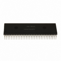
HD6473258P10V Renesas Electronics America, HD6473258P10V Datasheet - Page 86

HD6473258P10V
Manufacturer Part Number
HD6473258P10V
Description
MCU 5V 32K PB-FREE 64-DIP
Manufacturer
Renesas Electronics America
Series
H8® H8/325r
Specifications of HD6473258P10V
Core Size
8-Bit
Program Memory Size
32KB (32K x 8)
Oscillator Type
External
Core Processor
H8/300
Speed
10MHz
Connectivity
SCI, UART/USART
Number Of I /o
53
Program Memory Type
OTP
Ram Size
1K x 8
Voltage - Supply (vcc/vdd)
4.5 V ~ 5.5 V
Operating Temperature
-20°C ~ 75°C
Package / Case
64-DIP
No. Of I/o's
53
Ram Memory Size
1024Byte
Cpu Speed
10MHz
No. Of Timers
3
Digital Ic Case Style
DIP
Supply Voltage
RoHS Compliant
Controller Family/series
H8/330
Rohs Compliant
Yes
Lead Free Status / RoHS Status
Lead free / RoHS Compliant
Eeprom Size
-
Data Converters
-
Peripherals
-
Lead Free Status / RoHS Status
Lead free / RoHS Compliant
Available stocks
Company
Part Number
Manufacturer
Quantity
Price
Company:
Part Number:
HD6473258P10V
Manufacturer:
RENESAS
Quantity:
600
Part Number:
HD6473258P10V
Manufacturer:
HITACHI/日立
Quantity:
20 000
- Current page: 86 of 301
- Download datasheet (2Mb)
Section 5. I/O Ports
5.1 Overview
The H8/325 Series has seven parallel I/O ports, including:
• Five 8-bit input/output ports—ports 1, 2, 3, 4, and 7
• One 7-bit input/output port—port 6
• One 6-bit input/output port—port 5
All ports have programmable MOS input pull-ups. Ports 1 and 2 can drive LEDs.
Input and output are memory-mapped. The CPU views each port as a data register (DR) located in
the register field at the high end of the address space. Each port also has a data direction register
(DDR) which determines which pins are used for input and which for output.
Output: To send data to an output port, the CPU selects output in the data direction register and
writes the desired data in the data register, causing the data to be held in a latch. The latch output
drives the pin through a buffer amplifier. If the CPU reads the data register of an output port, it
obtains the data held in the latch rather than the actual level of the pin.
Input: To read data from an I/O port, the CPU selects input in the data direction register and reads
the data register. This causes the input logic level at the pin to be placed directly on the internal data
bus. There is no intervening input latch, except for port 3 when parallel handshaking is used.
MOS Pull-Up: The MOS pull-ups for input pins are controlled as follows. To turn on the pull-up
transistor for a pin, software must first clear its data direction bit to 0 to make the pin an input pin,
then write a 1 in the data bit for that pin. The pull-up can be turned off by writing a 0 in the data bit,
or a 1 in the data direction bit. The pull-ups are also turned off by a reset and by entry to the
hardware standby mode.
The data direction registers are write-only registers; their contents are invisible to the CPU. If the
CPU reads a data direction register all bits are read as 1, regardless of their true values. Care is
required if bit manipulation instructions are used to set and clear the data direction bits. See the
note on bit manipulation instructions in section 3.5.5, Bit Manipulations.
Auxiliary Functions: In addition to their general-purpose input/output functions, all of the I/O
ports have auxiliary functions. Most of the auxiliary functions are software-selectable and must be
enabled by setting bits in control registers. When selected, an auxiliary function usually replaces
the general-purpose input/output function, but in some cases both functions operate simultaneously.
Table 5-1 summarizes the auxiliary functions of the ports.
77
Related parts for HD6473258P10V
Image
Part Number
Description
Manufacturer
Datasheet
Request
R

Part Number:
Description:
KIT STARTER FOR M16C/29
Manufacturer:
Renesas Electronics America
Datasheet:

Part Number:
Description:
KIT STARTER FOR R8C/2D
Manufacturer:
Renesas Electronics America
Datasheet:

Part Number:
Description:
R0K33062P STARTER KIT
Manufacturer:
Renesas Electronics America
Datasheet:

Part Number:
Description:
KIT STARTER FOR R8C/23 E8A
Manufacturer:
Renesas Electronics America
Datasheet:

Part Number:
Description:
KIT STARTER FOR R8C/25
Manufacturer:
Renesas Electronics America
Datasheet:

Part Number:
Description:
KIT STARTER H8S2456 SHARPE DSPLY
Manufacturer:
Renesas Electronics America
Datasheet:

Part Number:
Description:
KIT STARTER FOR R8C38C
Manufacturer:
Renesas Electronics America
Datasheet:

Part Number:
Description:
KIT STARTER FOR R8C35C
Manufacturer:
Renesas Electronics America
Datasheet:

Part Number:
Description:
KIT STARTER FOR R8CL3AC+LCD APPS
Manufacturer:
Renesas Electronics America
Datasheet:

Part Number:
Description:
KIT STARTER FOR RX610
Manufacturer:
Renesas Electronics America
Datasheet:

Part Number:
Description:
KIT STARTER FOR R32C/118
Manufacturer:
Renesas Electronics America
Datasheet:

Part Number:
Description:
KIT DEV RSK-R8C/26-29
Manufacturer:
Renesas Electronics America
Datasheet:

Part Number:
Description:
KIT STARTER FOR SH7124
Manufacturer:
Renesas Electronics America
Datasheet:

Part Number:
Description:
KIT STARTER FOR H8SX/1622
Manufacturer:
Renesas Electronics America
Datasheet:

Part Number:
Description:
KIT DEV FOR SH7203
Manufacturer:
Renesas Electronics America
Datasheet:


