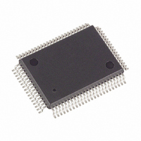
DS5002FMN-16 Maxim Integrated Products, DS5002FMN-16 Datasheet - Page 17

DS5002FMN-16
Manufacturer Part Number
DS5002FMN-16
Description
IC MPU SECURE 16MHZ IND 80-TQFP
Manufacturer
Maxim Integrated Products
Series
DS500xr
Datasheet
1.DS5002FPM-16.pdf
(25 pages)
Specifications of DS5002FMN-16
Core Processor
8051
Core Size
8-Bit
Speed
16MHz
Connectivity
EBI/EMI, SIO, UART/USART
Peripherals
Power-Fail Reset, WDT
Number Of I /o
32
Program Memory Type
SRAM
Ram Size
128 x 8
Voltage - Supply (vcc/vdd)
4.5 V ~ 5.5 V
Oscillator Type
External
Operating Temperature
-40°C ~ 85°C
Package / Case
80-MQFP, 80-PQFP
Processor Series
DS5002
Core
8051
Data Bus Width
8 bit
Program Memory Size
32 KB, 64 KB, 128 KB
Data Ram Size
32 KB, 64 KB, 128 KB
Interface Type
UART
Maximum Clock Frequency
16 MHz
Number Of Programmable I/os
32
Number Of Timers
2
Operating Supply Voltage
4.5 V to 5.5 V
Maximum Operating Temperature
+ 85 C
Mounting Style
SMD/SMT
3rd Party Development Tools
PK51, CA51, A51, ULINK2
Minimum Operating Temperature
- 40 C
Lead Free Status / RoHS Status
Contains lead / RoHS non-compliant
Eeprom Size
-
Program Memory Size
-
Data Converters
-
Available stocks
Company
Part Number
Manufacturer
Quantity
Price
Company:
Part Number:
DS5002FMN-16
Manufacturer:
Maxim Integrated
Quantity:
10 000
Company:
Part Number:
DS5002FMN-16+
Manufacturer:
Maxim Integrated Products
Quantity:
135
Company:
Part Number:
DS5002FMN-16+
Manufacturer:
Maxim Integrated
Quantity:
10 000
DS5002FP Secure Microprocessor Chip
protection measure, the address encryptor also generates “dummy” read access cycles whenever time is available
during program execution.
DUMMY READ CYCLES
Like the DS5000FP, the DS5002FP generates a “dummy” read access cycle to non-sequential addresses in
external RAM memory whenever time is available during program execution. This action has the affect of further
complicating the task of determining the normal flow of program execution. During these pseudorandom dummy
cycles, the RAM is read to all appearances, but the data is not used internally. Through the use of a repeatable
exchange of dummy and true read cycles, it is impossible to distinguish a dummy cycle from a real one.
ENCRYPTION ALGORITHM
The DS5002FP incorporates a proprietary algorithm implemented in hardware, which performs the scrambling of
address and data on the byte-wide bus to the SRAM. This algorithm has been greatly strengthened with respect to
its DS5000FP predecessor. Improvements include:
1) 64-bit encryption key
2) Incorporation of DES-like operations to provide a greater degree of nonlinearity
3) Customizable encryption
The encryption circuitry uses a 64-bit key value (compared to the DS5000FP’s 40-bit key), which is stored on the
DS5002FP die and protected by the Security Lock function described below. In addition, the algorithm has been
strengthened to incorporate certain operations used in DES encryption, so that the encryption of both the
addresses and data is highly nonlinear. Unlike the DS5000FP, the encryption circuitry in the DS5002FP is always
enabled.
Dallas Semiconductor can customize the encryption circuitry by laser programming the die to insure that a unique
encryption algorithm is delivered to the customer. In addition, the customer-specific version can be branded as
specified by the customer. Please contact Dallas Semiconductor for ordering information of customer-specific
versions.
ENCRYPTION KEY
As described above, the on-chip 64-bit encryption key is the basis of both the address and data encryptor circuits.
The DS5002FP provides a key management system, which is greatly improved over the DS5000FP. The
DS5002FP does not give the user the ability to select a key. Instead, when the loader is given certain commands,
the key is set based on the value read from an on-chip hardware random number generator. This action is
performed just prior to actually loading the code into the external RAM. This scheme prevents characterization of
the encryption algorithm by continuously loading new, known keys. It also frees the user from the burden of
protecting the key selection process.
The random number generator circuit uses the asynchronous frequency differences of two internal ring oscillator
and the processor master clock (determined by XTAL1 and XTAL2). As a result, a true random number is
produced.
VECTOR RAM
A 48-byte vector RAM area is incorporated on-chip, and is used to contain the reset and interrupt vector code in the
DS5002FP. It is included in the architecture to help insure the security of the application program.
If reset and interrupt vector locations were accessed from the external nonvolatile program/data RAM during the
execution of the program, then it would be possible to determine the encrypted value of known addresses. This
could be done by forcing an interrupt or reset condition and observing the resulting addresses on the byte-wide
address/data bus. For example, it is known that when a hardware reset is applied the logical program address is
forced to location 0000H and code is executed starting from this location. It would then be possible to determine
the encrypted value (or physical address) of the logical address value 0000H by observing the address presented
to the external RAM following a hardware reset. Interrupt vector address relationships could be determined in a
similar fashion. By using the on-chip vector RAM to contain the interrupt and reset vectors, it is impossible to
17 of 25


