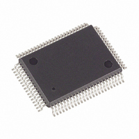
DS5002FMN-16 Maxim Integrated Products, DS5002FMN-16 Datasheet - Page 8

DS5002FMN-16
Manufacturer Part Number
DS5002FMN-16
Description
IC MPU SECURE 16MHZ IND 80-TQFP
Manufacturer
Maxim Integrated Products
Series
DS500xr
Datasheet
1.DS5002FPM-16.pdf
(25 pages)
Specifications of DS5002FMN-16
Core Processor
8051
Core Size
8-Bit
Speed
16MHz
Connectivity
EBI/EMI, SIO, UART/USART
Peripherals
Power-Fail Reset, WDT
Number Of I /o
32
Program Memory Type
SRAM
Ram Size
128 x 8
Voltage - Supply (vcc/vdd)
4.5 V ~ 5.5 V
Oscillator Type
External
Operating Temperature
-40°C ~ 85°C
Package / Case
80-MQFP, 80-PQFP
Processor Series
DS5002
Core
8051
Data Bus Width
8 bit
Program Memory Size
32 KB, 64 KB, 128 KB
Data Ram Size
32 KB, 64 KB, 128 KB
Interface Type
UART
Maximum Clock Frequency
16 MHz
Number Of Programmable I/os
32
Number Of Timers
2
Operating Supply Voltage
4.5 V to 5.5 V
Maximum Operating Temperature
+ 85 C
Mounting Style
SMD/SMT
3rd Party Development Tools
PK51, CA51, A51, ULINK2
Minimum Operating Temperature
- 40 C
Lead Free Status / RoHS Status
Contains lead / RoHS non-compliant
Eeprom Size
-
Program Memory Size
-
Data Converters
-
Available stocks
Company
Part Number
Manufacturer
Quantity
Price
Company:
Part Number:
DS5002FMN-16
Manufacturer:
Maxim Integrated
Quantity:
10 000
Company:
Part Number:
DS5002FMN-16+
Manufacturer:
Maxim Integrated Products
Quantity:
135
Company:
Part Number:
DS5002FMN-16+
Manufacturer:
Maxim Integrated
Quantity:
10 000
AC CHARACTERISTICS—BYTE-WIDE ADDRESS/DATA BUS TIMING
(V
Figure 6. Byte-Wide Bus Timing
CC
40
41
42
43
44
45
46
47
48
49
50
51
52
53
#
= 5V ±10%, T
Delay to Byte-Wide Address Valid from CE1 ,
CE2 , or CE1N Low During Op Code Fetch
Pulse Width of CE 1–4, PE 1–4, or CE1N
Byte-Wide Address Hold After CE1 , CE2 , or
CE1N High During Op Code Fetch
Byte-Wide Data Setup to CE1 , CE2 , or CE1N
High During Op Code Fetch
Byte-Wide Data Hold After CE1 , CE2 , or CE1N
High During Op Code Fetch
Byte-Wide Address Hold After CE 1–4, PE 1–4, or
CE1N High During MOVX
Delay from Byte-Wide Address Valid CE 1–4,
PE 1–4, or CE1N Low During MOVX
Byte-Wide Data Setup to CE 1–4, PE 1–4, or
CE1N High During MOVX (Read)
Byte-Wide Data Hold After CE 1–4, PE 1–4, or
CE1N High During MOVX (Read)
Byte-Wide Address Valid to R/ W Active During
MOVX (Write)
Delay from R/ W Low to Valid Data Out During
MOVX (Write)
Valid Data Out Hold Time from CE 1–4, PE 1–4, or
CE1N High
Valid Data Out Hold Time from R/ W High
Write Pulse Width (R/ W Low Time)
A
= 0°C to +70°C.)
PARAMETER
(Figure
6)
8 of 25
SYMBOL
t
t
t
t
t
t
t
t
t
t
t
t
OVCE1H
CE1HOV
t
CE1HPA
CE1LPA
t
RWHDV
RWLPW
AVRWL
RWLDV
CEHDA
DACEH
CEHDV
CEHDV
CELDA
CEPW
1t
1t
4t
2t
4t
4t
3t
1t
6t
CLK
CLK
CLK
CLK
CLK
CLK
CLK
CLK
CLK
MIN
20
0
0
0
+ 40
+ 40
- 35
- 20
- 30
- 35
- 35
- 15
- 20
MAX
30
UNITS
ns
ns
ns
ns
ns
ns
ns
ns
ns
ns
ns
ns
ns
ns


