PIC18C242/JW Microchip Technology, PIC18C242/JW Datasheet - Page 163
PIC18C242/JW
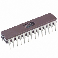
Manufacturer Part Number
PIC18C242/JW
Description
IC MCU EPROM 8KX16 A/D 28CDIP
Manufacturer
Microchip Technology
Series
PIC® 18Cr
Datasheets
1.PIC16F616T-ISL.pdf
(8 pages)
2.PIC16C770-ISO.pdf
(8 pages)
3.PIC18C242-ISO.pdf
(305 pages)
4.PIC18C242-ISO.pdf
(12 pages)
Specifications of PIC18C242/JW
Core Processor
PIC
Core Size
8-Bit
Speed
40MHz
Connectivity
I²C, SPI, UART/USART
Peripherals
Brown-out Detect/Reset, LVD, POR, PWM, WDT
Number Of I /o
22
Program Memory Size
16KB (8K x 16)
Program Memory Type
EPROM, UV
Ram Size
512 x 8
Voltage - Supply (vcc/vdd)
4.2 V ~ 5.5 V
Data Converters
A/D 5x10b
Oscillator Type
External
Operating Temperature
0°C ~ 70°C
Package / Case
28-CDIP (0.300", 7.62mm) Window
Lead Free Status / RoHS Status
Contains lead / RoHS non-compliant
Eeprom Size
-
Available stocks
Company
Part Number
Manufacturer
Quantity
Price
Company:

Part Number:
PIC18C242/JW
Manufacturer:
NS
Quantity:
10


15.3.2
Once Synchronous mode is selected, reception is
enabled
(RCSTA<5>), or enable bit CREN (RCSTA<4>). Data is
sampled on the RC7/RX/DT pin on the falling edge of
the clock. If enable bit SREN is set, only a single word
is received. If enable bit CREN is set, the reception is
continuous until CREN is cleared. If both bits are set,
then CREN takes precedence.
To set up a Synchronous Master Reception:
1.
2.
TABLE 15-9:
FIGURE 15-8:
INTCON
PIR1
PIE1
IPR1
RCSTA
RCREG
TXSTA
SPBRG
Legend: x = unknown, - = unimplemented, read as '0'.
Note 1: The PSPIF, PSPIE and PSPIP bits are reserved on the PIC18C2X2 devices. Always maintain these bits
2001 Microchip Technology Inc.
Name
RC7/RX/DT pin
RC6/TX/CK pin
Initialize the SPBRG register for the appropriate
baud rate (Section 15.1).
Enable the synchronous master serial port by
setting bits SYNC, SPEN and CSRC.
Note:
(interrupt)
Write to
bit SREN
SREN bit
CREN bit
Shaded cells are not used for Synchronous Master Reception.
RCIF bit
RXREG
by
clear.
Read
USART SYNCHRONOUS MASTER
RECEPTION
USART Receive Register
Baud Rate Generator Register
PSPIF
PSPIE
PSPIP
Timing diagram demonstrates Sync Master mode with bit SREN = ’1’ and bit BRGH = ’0’.
CSRC
SPEN
GIEH
Bit 7
GIE/
setting
Q2
REGISTERS ASSOCIATED WITH SYNCHRONOUS MASTER RECEPTION
(1)
(1)
(1)
’0’
Q3 Q4 Q1 Q2 Q3 Q4 Q1 Q2 Q3 Q4
SYNCHRONOUS RECEPTION (MASTER MODE, SREN)
PEIE/
GIEL
ADIF
ADIE
ADIP
Bit 6
RX9
TX9
either
TMR0IE INT0IE
SREN
TXEN
bit0
RCIF
RCIE
RCIP
enable
Bit 5
Q1 Q2 Q3 Q4 Q1 Q2 Q3 Q4 Q1 Q2 Q3 Q4 Q1 Q2 Q3 Q4 Q1 Q2 Q3 Q4 Q1 Q2 Q3 Q4 Q1 Q2 Q3 Q4
bit1
CREN ADDEN
SYNC
bit
Bit 4
TXIF
TXIE
TXIP
SREN
bit2
SSPIF
SSPIE
SSPIP
RBIE
Bit 3
—
bit3
TMR0IF INT0IF
CCP1IF TMR2IF TMR1IF 0000 0000 0000 0000
CCP1IE TMR2IE TMR1IE 0000 0000 0000 0000
CCP1IP TMR2IP TMR1IP 0000 0000 0000 0000
BRGH
FERR
Bit 2
3.
4.
5.
6.
7.
8.
9.
10. If any error occurred, clear the error by clearing
Ensure bits CREN and SREN are clear.
If interrupts are desired, set enable bit RCIE.
If 9-bit reception is desired, set bit RX9.
If a single reception is required, set bit SREN.
For continuous reception, set bit CREN.
Interrupt flag bit RCIF will be set when reception
is complete and an interrupt will be generated if
the enable bit RCIE was set.
Read the RCSTA register to get the ninth bit (if
enabled) and determine if any error occurred
during reception.
Read the 8-bit received data by reading the
RCREG register.
bit CREN.
bit4
OERR
TRMT
Bit 1
bit5
RX9D
TX9D
RBIF
Bit 0
bit6
PIC18CXX2
0000 000x 0000 000u
0000 -00x 0000 -00x
0000 0000 0000 0000
0000 -010 0000 -010
0000 0000 0000 0000
Value on
POR,
BOR
bit7
DS39026C-page 161
Value on all
Q1 Q2 Q3 Q4
RESETS
other
’0’
Related parts for PIC18C242/JW
Image
Part Number
Description
Manufacturer
Datasheet
Request
R

Part Number:
Description:
IC, 8BIT MCU, PIC18F, 40MHZ, LCC-44
Manufacturer:
Microchip Technology
Datasheet:
Part Number:
Description:
IC, 8BIT MCU, PIC18LF, 40MHZ, PLCC-64
Manufacturer:
Microchip Technology
Datasheet:
Part Number:
Description:
IC, 8BIT MCU, PIC18F, 64MHZ, TQFP-80
Manufacturer:
Microchip Technology
Datasheet:

Part Number:
Description:
MCU, MPU & DSP Development Tools CAN/LIN PICtail Plus Daughter Board
Manufacturer:
Microchip Technology
Datasheet:

Part Number:
Description:
IC, 8BIT MCU, PIC18F, 64MHZ, DIP-40
Manufacturer:
Microchip Technology
Datasheet:

Part Number:
Description:
IC, 8BIT MCU, PIC18LF, 40MHZ, PLCC-64
Manufacturer:
Microchip Technology
Datasheet:
Part Number:
Description:
IC, 8BIT MCU, PIC18F, 64MHZ, TQFP-64
Manufacturer:
Microchip Technology
Part Number:
Description:
IC, 8BIT MCU, PIC18F, 64MHZ, TQFP-80
Manufacturer:
Microchip Technology

Part Number:
Description:
8KB, Flash, 768bytes-RAM, 36I/O, 8-bit Family,nanowatt XLP 40 UQFN 5x5x0.5mm TUB
Manufacturer:
Microchip Technology
Datasheet:
Part Number:
Description:
8KB, Flash, 768bytes-RAM, 36I/O, 8-bit Family,nanowatt XLP 40 UQFN 5x5x0.5mm TUB
Manufacturer:
Microchip Technology
Part Number:
Description:
16KB, Flash, 768bytes-RAM, 36I/O, 8-bit Family,nanowatt XLP 40 UQFN 5x5x0.5mm TU
Manufacturer:
Microchip Technology
Datasheet:
Part Number:
Description:
16KB, Flash, 768bytes-RAM, 36I/O, 8-bit Family,nanowatt XLP 40 UQFN 5x5x0.5mm TU
Manufacturer:
Microchip Technology
Part Number:
Description:
32KB, Flash, 1536bytes-RAM, 36I/O, 8-bit Family,nanowatt XLP 40 UQFN 5x5x0.5mm T
Manufacturer:
Microchip Technology
Datasheet:
Part Number:
Description:
32KB, Flash, 1536bytes-RAM, 36I/O, 8-bit Family,nanowatt XLP 40 UQFN 5x5x0.5mm T
Manufacturer:
Microchip Technology
Part Number:
Description:
64KB, Flash, 3968bytes-RAM, 36I/O, 8-bit Family,nanowatt XLP 40 UQFN 5x5x0.5mm T
Manufacturer:
Microchip Technology
Datasheet: