PIC18C242/JW Microchip Technology, PIC18C242/JW Datasheet - Page 294
PIC18C242/JW
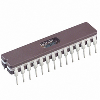
Manufacturer Part Number
PIC18C242/JW
Description
IC MCU EPROM 8KX16 A/D 28CDIP
Manufacturer
Microchip Technology
Series
PIC® 18Cr
Datasheets
1.PIC16F616T-ISL.pdf
(8 pages)
2.PIC16C770-ISO.pdf
(8 pages)
3.PIC18C242-ISO.pdf
(305 pages)
4.PIC18C242-ISO.pdf
(12 pages)
Specifications of PIC18C242/JW
Core Processor
PIC
Core Size
8-Bit
Speed
40MHz
Connectivity
I²C, SPI, UART/USART
Peripherals
Brown-out Detect/Reset, LVD, POR, PWM, WDT
Number Of I /o
22
Program Memory Size
16KB (8K x 16)
Program Memory Type
EPROM, UV
Ram Size
512 x 8
Voltage - Supply (vcc/vdd)
4.2 V ~ 5.5 V
Data Converters
A/D 5x10b
Oscillator Type
External
Operating Temperature
0°C ~ 70°C
Package / Case
28-CDIP (0.300", 7.62mm) Window
Lead Free Status / RoHS Status
Contains lead / RoHS non-compliant
Eeprom Size
-
Available stocks
Company
Part Number
Manufacturer
Quantity
Price
Company:

Part Number:
PIC18C242/JW
Manufacturer:
NS
Quantity:
10


PIC18CXX2
Code Examples
Code Protection ....................................................... 179, 186
COMF ............................................................................... 204
Compare (CCP Module) ................................................... 110
Configuration Bits ............................................................. 179
Context Saving During Interrupts ....................................... 75
Conversion Considerations .............................................. 288
CPFSEQ .......................................................................... 204
CPFSGT ........................................................................... 205
CPFSLT ........................................................................... 205
D
Data Memory ...................................................................... 42
DAW ................................................................................. 206
DC Characteristics ................................................... 237, 240
DECF ............................................................................... 206
DECFSNZ ........................................................................ 207
DECFSZ ........................................................................... 207
Device Differences ........................................................... 287
Direct Addressing ............................................................... 51
E
Electrical Characteristics .................................................. 235
Errata ................................................................................... 5
F
Firmware Instructions ....................................................... 187
G
General Call Address Sequence ...................................... 133
General Call Address Support ......................................... 133
GOTO ............................................................................... 208
DS39026C-page 292
16 x 16 Signed Multiply Routine ................................ 62
16 x 16 Unsigned Multiply Routine ............................ 62
8 x 8 Signed Multiply Routine .................................... 61
8 x 8 Unsigned Multiply Routine ................................ 61
Changing Between Capture Prescalers ................... 109
Fast Register Stack .................................................... 39
Initializing PORTA ...................................................... 77
Initializing PORTB ...................................................... 80
Initializing PORTC ...................................................... 83
Initializing PORTD ...................................................... 85
Initializing PORTE ...................................................... 87
Loading the SSPBUF Register ................................ 122
Saving STATUS, WREG and BSR Registers
Associated Registers ............................................... 111
Block Diagram .......................................................... 110
CCP Pin Configuration ............................................. 110
CCPR1H:CCPR1L Registers ................................... 110
Software Interrupt .................................................... 110
Special Event Trigger ......................... 99, 105, 110, 171
Timer1 Mode Selection ............................................ 110
Example Code ........................................................... 75
General Purpose Registers ........................................ 42
Special Function Registers ........................................ 42
in RAM ............................................................... 75
I
I/O Ports ............................................................................. 77
I
I
I
I
ICEPIC In-Circuit Emulator .............................................. 230
ID Locations ............................................................. 179, 186
INCF ................................................................................ 208
INCFSZ ............................................................................ 209
In-Circuit Serial Programming (ICSP) ...................... 179, 186
Indirect Addressing ............................................................ 51
INFSNZ ............................................................................ 209
Instruction Cycle ................................................................ 39
Instruction Flow/Pipelining ................................................. 40
Instruction Format ............................................................ 189
2
2
2
2
C (SSP Module) ............................................................ 128
C Master Mode Reception ............................................ 139
C Master Mode Repeated START Condition ................ 138
C Module
ACK Pulse ....................................................... 128, 129
Addressing ............................................................... 129
Block Diagram ......................................................... 128
Read/Write Bit Information (R/W Bit) ....................... 129
Reception ................................................................ 129
Serial Clock (RC3/SCK/SCL) ................................... 129
Slave Mode .............................................................. 128
Timing Diagram, Data .............................................. 257
Timing Diagram, START/STOP Bits ........................ 256
Transmission ........................................................... 129
Acknowledge Sequence Timing .............................. 142
Baud Rate Generator
Block Diagram
BRG Reset Due to SDA Collision ............................ 146
BRG Timing ............................................................. 136
Bus Collision
Bus Collision Timing ................................................ 144
Clock Arbitration ...................................................... 143
Clock Arbitration Timing (Master Transmit) ............. 143
General Call Address Support ................................. 133
Master Mode 7-bit Reception Timing ....................... 141
Master Mode Operation ........................................... 135
Master Mode START Condition ............................... 137
Master Mode Transmission ..................................... 139
Master Mode Transmit Sequence ............................ 135
Multi-Master Mode ................................................... 144
Repeat START Condition Timing ............................ 138
STOP Condition Receive or Transmit Timing .......... 143
STOP Condition Timing ........................................... 142
Waveforms for 7-bit Reception ................................ 130
Waveforms for 7-bit Transmission ........................... 130
FSR Register ............................................................. 50
Baud Rate Generator ...................................... 136
Acknowledge ................................................... 144
Repeated START Condition ............................ 147
Repeated START Condition Timing
Repeated START Condition Timing
START Condition ............................................. 145
START Condition Timing ......................... 145, 146
STOP Condition ............................................... 148
STOP Condition Timing (Case 1) .................... 148
STOP Condition Timing (Case 2) .................... 148
Transmit Timing ............................................... 144
(Case 1) ................................................... 147
(Case 2) ................................................... 147
2001 Microchip Technology Inc.
Related parts for PIC18C242/JW
Image
Part Number
Description
Manufacturer
Datasheet
Request
R

Part Number:
Description:
IC, 8BIT MCU, PIC18F, 40MHZ, LCC-44
Manufacturer:
Microchip Technology
Datasheet:
Part Number:
Description:
IC, 8BIT MCU, PIC18LF, 40MHZ, PLCC-64
Manufacturer:
Microchip Technology
Datasheet:
Part Number:
Description:
IC, 8BIT MCU, PIC18F, 64MHZ, TQFP-80
Manufacturer:
Microchip Technology
Datasheet:

Part Number:
Description:
MCU, MPU & DSP Development Tools CAN/LIN PICtail Plus Daughter Board
Manufacturer:
Microchip Technology
Datasheet:

Part Number:
Description:
IC, 8BIT MCU, PIC18F, 64MHZ, DIP-40
Manufacturer:
Microchip Technology
Datasheet:

Part Number:
Description:
IC, 8BIT MCU, PIC18LF, 40MHZ, PLCC-64
Manufacturer:
Microchip Technology
Datasheet:
Part Number:
Description:
IC, 8BIT MCU, PIC18F, 64MHZ, TQFP-64
Manufacturer:
Microchip Technology
Part Number:
Description:
IC, 8BIT MCU, PIC18F, 64MHZ, TQFP-80
Manufacturer:
Microchip Technology

Part Number:
Description:
8KB, Flash, 768bytes-RAM, 36I/O, 8-bit Family,nanowatt XLP 40 UQFN 5x5x0.5mm TUB
Manufacturer:
Microchip Technology
Datasheet:
Part Number:
Description:
8KB, Flash, 768bytes-RAM, 36I/O, 8-bit Family,nanowatt XLP 40 UQFN 5x5x0.5mm TUB
Manufacturer:
Microchip Technology
Part Number:
Description:
16KB, Flash, 768bytes-RAM, 36I/O, 8-bit Family,nanowatt XLP 40 UQFN 5x5x0.5mm TU
Manufacturer:
Microchip Technology
Datasheet:
Part Number:
Description:
16KB, Flash, 768bytes-RAM, 36I/O, 8-bit Family,nanowatt XLP 40 UQFN 5x5x0.5mm TU
Manufacturer:
Microchip Technology
Part Number:
Description:
32KB, Flash, 1536bytes-RAM, 36I/O, 8-bit Family,nanowatt XLP 40 UQFN 5x5x0.5mm T
Manufacturer:
Microchip Technology
Datasheet:
Part Number:
Description:
32KB, Flash, 1536bytes-RAM, 36I/O, 8-bit Family,nanowatt XLP 40 UQFN 5x5x0.5mm T
Manufacturer:
Microchip Technology
Part Number:
Description:
64KB, Flash, 3968bytes-RAM, 36I/O, 8-bit Family,nanowatt XLP 40 UQFN 5x5x0.5mm T
Manufacturer:
Microchip Technology
Datasheet: