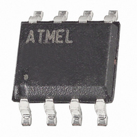
ATTINY12-8SI Atmel, ATTINY12-8SI Datasheet - Page 6

ATTINY12-8SI
Manufacturer Part Number
ATTINY12-8SI
Description
IC AVR MCU 1K 5V 8MHZ IND SO-8
Manufacturer
Atmel
Series
AVR® ATtinyr
Specifications of ATTINY12-8SI
Core Processor
AVR
Core Size
8-Bit
Speed
8MHz
Peripherals
POR, WDT
Number Of I /o
6
Program Memory Size
1KB (512 x 16)
Program Memory Type
FLASH
Eeprom Size
64 x 8
Voltage - Supply (vcc/vdd)
4 V ~ 5.5 V
Oscillator Type
Internal
Operating Temperature
-40°C ~ 85°C
Package / Case
8-SOIC (5.3mm Width), 8-SOP, 8-SOEIAJ
Data Bus Width
8 bit
Maximum Clock Frequency
8 MHz
Number Of Programmable I/os
12
Number Of Timers
1 x 8 bit
Operating Supply Voltage
4 V to 5.5 V
Maximum Operating Temperature
+ 85 C
Mounting Style
SMD/SMT
Minimum Operating Temperature
- 55 C
Lead Free Status / RoHS Status
Contains lead / RoHS non-compliant
Ram Size
-
Data Converters
-
Connectivity
-
Lead Free Status / Rohs Status
No
Other names
ATTINY128SI
Available stocks
Company
Part Number
Manufacturer
Quantity
Price
Company:
Part Number:
ATTINY12-8SI
Manufacturer:
ATMEL
Quantity:
1 729
Architectural
Overview
6
ATtiny11/12
The fast-access register file concept contains 32 x 8-bit general-purpose working regis-
ters with a single-clock-cycle access time. This means that during one single clock
cycle, one ALU (Arithmetic Logic Unit) operation is executed. Two operands are output
from the register file, the operation is executed, and the result is stored back in the reg-
ister file – in one clock cycle.
Two of the 32 registers can be used as a 16-bit pointer for indirect memory access. This
pointer is called the Z-pointer, and can address the register file and the Flash program
memory.
The ALU supports arithmetic and logic functions between registers or between a con-
stant and a register. Single-register operations are also executed in the ALU. Figure 2
shows the ATtiny11/12 AVR RISC microcontroller architecture. The AVR uses a Har-
vard architecture concept with separate memories and buses for program and data
memories. The program memory is accessed with a two-stage pipelining. While one
instruction is being executed, the next instruction is pre-fetched from the program mem-
ory. This concept enables instructions to be executed in every clock cycle. The program
memory is reprogrammable Flash memory.
With the relative jump and relative call instructions, the whole 512 address space is
directly accessed. All AVR instructions have a single 16-bit word format, meaning that
every program memory address contains a single 16-bit instruction.
During interrupts and subroutine calls, the return address program counter (PC) is
stored on the stack. The stack is a 3-level-deep hardware stack dedicated for subrou-
tines and interrupts.
The I/O memory space contains 64 addresses for CPU peripheral functions as control
registers, timer/counters, and other I/O functions. The memory spaces in the AVR archi-
tecture are all linear and regular memory maps.
1006F–AVR–06/07


