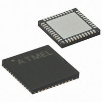
ATMEGA8535L-8MI Atmel, ATMEGA8535L-8MI Datasheet - Page 90

ATMEGA8535L-8MI
Manufacturer Part Number
ATMEGA8535L-8MI
Description
IC AVR MCU 8K LV 8MHZ IND 44-QFN
Manufacturer
Atmel
Series
AVR® ATmegar
Specifications of ATMEGA8535L-8MI
Core Processor
AVR
Core Size
8-Bit
Speed
8MHz
Connectivity
I²C, SPI, UART/USART
Peripherals
Brown-out Detect/Reset, POR, PWM, WDT
Number Of I /o
32
Program Memory Size
8KB (4K x 16)
Program Memory Type
FLASH
Eeprom Size
512 x 8
Ram Size
512 x 8
Voltage - Supply (vcc/vdd)
2.7 V ~ 5.5 V
Data Converters
A/D 8x10b
Oscillator Type
Internal
Operating Temperature
-40°C ~ 85°C
Package / Case
44-VQFN Exposed Pad
Data Bus Width
8 bit
Data Ram Size
512 B
Interface Type
SPI, TWI, UART
Maximum Clock Frequency
8 MHz
Number Of Programmable I/os
32
Number Of Timers
3
Operating Supply Voltage
2.7 V to 5.5 V
Maximum Operating Temperature
+ 85 C
Mounting Style
SMD/SMT
Minimum Operating Temperature
- 40 C
On-chip Adc
10 bit, 8 Channel
Lead Free Status / RoHS Status
Contains lead / RoHS non-compliant
Available stocks
Company
Part Number
Manufacturer
Quantity
Price
Company:
Part Number:
ATMEGA8535L-8MI
Manufacturer:
SanRex
Quantity:
1 000
- Current page: 90 of 321
- Download datasheet (3Mb)
Registers
90
ATmega8535(L)
Figure 40. 16-bit Timer/Counter Block Diagram
Note:
The Timer/Counter (TCNT1), Output Compare Registers (OCR1A/B), and Input Capture
Register (ICR1) are all 16-bit registers. Special procedures must be followed when
accessing the 16-bit registers. These procedures are described in the section “Access-
ing 16-bit Registers” on page 92. The Timer/Counter Control Registers (TCCR1A/B) are
8-bit registers and have no CPU access restrictions. Interrupt requests (abbreviated to
Int.Req. in the figure) signals are all visible in the Timer Interrupt Flag Register (TIFR).
All interrupts are individually masked with the Timer Interrupt Mask Register (TIMSK).
TIFR and TIMSK are not shown in the figure since these registers are shared by other
timer units.
The Timer/Counter can be clocked internally, via the prescaler, or by an external clock
source on the T1 pin. The Clock Select logic block controls which clock source and edge
the Timer/Counter uses to increment (or decrement) its value. The Timer/Counter is
inactive when no clock source is selected. The output from the Clock Select logic is
referred to as the timer clock (clk
The double buffered Output Compare Registers (OCR1A/B) are compared with the
Timer/Counter value at all times. The result of the compare can be used by the
1. Refer to Figure 1 on page 2, Table 26 on page 60, and Table 32 on page 64 for
Timer/Counter1 pin placement and description.
Timer/Counter
TCCRnA
OCRnA
OCRnB
TCNTn
ICRn
=
=
Direction
Count
Clear
Control Logic
T
1
TOP
).
=
TCCRnB
Values
BOTTOM
Fixed
TOP
ICFn (Int.Req.)
clk
Detector
Edge
=
Tn
0
(1)
OCnA
(Int.Req.)
OCnB
(Int.Req.)
TOVn
(Int.Req.)
Clock Select
Generation
Generation
Waveform
Waveform
( From Prescaler )
Canceler
Detector
Noise
Edge
Comparator Ouput )
( From Analog
2502K–AVR–10/06
OCnA
OCnB
ICPn
Tn
Related parts for ATMEGA8535L-8MI
Image
Part Number
Description
Manufacturer
Datasheet
Request
R

Part Number:
Description:
IC AVR MCU 2.4GHZ XCEIVER 64QFN
Manufacturer:
Atmel
Datasheet:

Part Number:
Description:
Manufacturer:
Atmel
Datasheet:

Part Number:
Description:
MCU ATMEGA644/AT86RF230 40-DIP
Manufacturer:
Atmel
Datasheet:

Part Number:
Description:
BUNDLE ATMEGA644P/AT86RF230 QFN
Manufacturer:
Atmel
Datasheet:

Part Number:
Description:
BUNDLE ATMEGA644P/AT86RF230 TQFP
Manufacturer:
Atmel
Datasheet:

Part Number:
Description:
MCU ATMEGA1281/AT86RF230 64-TQFP
Manufacturer:
Atmel
Datasheet:

Part Number:
Description:
MCU ATMEGA1280/AT86RF230 100TQFP
Manufacturer:
Atmel
Datasheet:

Part Number:
Description:
BUNDLE ATMEGA1280/AT86RF100-TQFP
Manufacturer:
Atmel
Datasheet:

Part Number:
Description:
BUNDLE ATMEGA2560V/AT86RF230-ZU
Manufacturer:
Atmel
Datasheet:

Part Number:
Description:
MCU ATMEGA2561/AT86RF230 64-TQFP
Manufacturer:
Atmel
Datasheet:

Part Number:
Description:
INTERVAL AND WIPE/WASH WIPER CONTROL IC WITH DELAY
Manufacturer:
ATMEL Corporation
Datasheet:

Part Number:
Description:
Low-Voltage Voice-Switched IC for Hands-Free Operation
Manufacturer:
ATMEL Corporation
Datasheet:

Part Number:
Description:
MONOLITHIC INTEGRATED FEATUREPHONE CIRCUIT
Manufacturer:
ATMEL Corporation
Datasheet:

Part Number:
Description:
AM-FM Receiver IC U4255BM-M
Manufacturer:
ATMEL Corporation
Datasheet:


