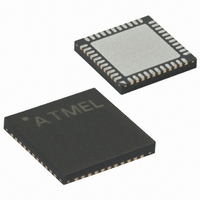
ATMEGA164P-15MT1 Atmel, ATMEGA164P-15MT1 Datasheet - Page 142

ATMEGA164P-15MT1
Manufacturer Part Number
ATMEGA164P-15MT1
Description
MCU AVR 16K FLASH 15MHZ 44-QFN
Manufacturer
Atmel
Series
AVR® ATmegar
Specifications of ATMEGA164P-15MT1
Core Processor
AVR
Core Size
8-Bit
Speed
16MHz
Connectivity
I²C, SPI, UART/USART
Peripherals
Brown-out Detect/Reset, POR, PWM, WDT
Number Of I /o
32
Program Memory Size
16KB (8K x 16)
Program Memory Type
FLASH
Eeprom Size
512 x 8
Ram Size
1K x 8
Voltage - Supply (vcc/vdd)
2.7 V ~ 5.5 V
Data Converters
A/D 8x10b
Oscillator Type
Internal
Operating Temperature
-40°C ~ 105°C
Package / Case
44-VQFN
Lead Free Status / RoHS Status
Lead free / RoHS Compliant
- Current page: 142 of 377
- Download datasheet (7Mb)
15.5
15.5.1
142
Output Compare Unit
ATmega164P/324P/644P
Force Output Compare
The 8-bit comparator continuously compares TCNT2 with the Output Compare Register
(OCR2A and OCR2B). Whenever TCNT2 equals OCR2A or OCR2B, the comparator signals a
match. A match will set the Output Compare Flag (OCF2A or OCF2B) at the next timer clock
cycle. If the corresponding interrupt is enabled, the Output Compare Flag generates an Output
Compare interrupt. The Output Compare Flag is automatically cleared when the interrupt is exe-
cuted. Alternatively, the Output Compare Flag can be cleared by software by writing a logical
one to its I/O bit location. The Waveform Generator uses the match signal to generate an output
according to operating mode set by the WGM22:0 bits and Compare Output mode (COM2x1:0)
bits. The max and bottom signals are used by the Waveform Generator for handling the special
cases of the extreme values in some modes of operation
Figure 14-10 on page 130
Figure 15-3. Output Compare Unit, Block Diagram
The OCR2x Register is double buffered when using any of the Pulse Width Modulation (PWM)
modes. For the Normal and Clear Timer on Compare (CTC) modes of operation, the double
buffering is disabled. The double buffering synchronizes the update of the OCR2x Compare
Register to either top or bottom of the counting sequence. The synchronization prevents the
occurrence of odd-length, non-symmetrical PWM pulses, thereby making the output glitch-free.
The OCR2x Register access may seem complex, but this is not case. When the double buffering
is enabled, the CPU has access to the OCR2x Buffer Register, and if double buffering is dis-
abled the CPU will access the OCR2x directly.
In non-PWM waveform generation modes, the match output of the comparator can be forced by
writing a one to the Force Output Compare (FOC2x) bit. Forcing compare match will not set the
OCF2x Flag or reload/clear the timer, but the OC2x pin will be updated as if a real compare
match had occurred (the COM2x1:0 bits settings define whether the OC2x pin is set, cleared or
toggled).
bottom
FOCn
top
OCRnx
shows a block diagram of the Output Compare unit.
Waveform Generator
WGMn1:0
=
(8-bit Comparator )
DATA BUS
COMnX1:0
(“Modes of Operation” on page
TCNTn
OCFnx (Int.Req.)
OCnx
7674F–AVR–09/09
145).
Related parts for ATMEGA164P-15MT1
Image
Part Number
Description
Manufacturer
Datasheet
Request
R

Part Number:
Description:
Manufacturer:
Atmel Corporation
Datasheet:

Part Number:
Description:
Manufacturer:
Atmel Corporation
Datasheet:

Part Number:
Description:
IC MCU AVR 16K FLASH 44-TQFP
Manufacturer:
Atmel
Datasheet:

Part Number:
Description:
IC MCU AVR 16K FLASH 44-QFN
Manufacturer:
Atmel
Datasheet:

Part Number:
Description:
MCU AVR 16K FLASH 20MHZ 44-TQFP
Manufacturer:
Atmel
Datasheet:

Part Number:
Description:
MCU AVR 16KB FLASH 15MHZ 44TQFP
Manufacturer:
Atmel
Datasheet:

Part Number:
Description:
IC MCU AVR 16K FLASH 40-DIP
Manufacturer:
Atmel
Datasheet:

Part Number:
Description:
MCU AVR 16KB FLASH 20MHZ 44-VQFN
Manufacturer:
Atmel
Datasheet:

Part Number:
Description:
MCU AVR 16KB FLASH 20MHZ 44TQFP
Manufacturer:
Atmel
Datasheet:

Part Number:
Description:
MCU AVR 16K FLASH 20MHZ 44-QFN
Manufacturer:
Atmel
Datasheet:

Part Number:
Description:
MCU AVR 16K FLASH 20MHZ 40-PDIP
Manufacturer:
Atmel
Datasheet:

Part Number:
Description:
MCU AVR 16KB FLASH 15MHZ 44TQFP
Manufacturer:
Atmel
Datasheet:


