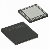
ATMEGA164P-15MT1 Atmel, ATMEGA164P-15MT1 Datasheet - Page 275

ATMEGA164P-15MT1
Manufacturer Part Number
ATMEGA164P-15MT1
Description
MCU AVR 16K FLASH 15MHZ 44-QFN
Manufacturer
Atmel
Series
AVR® ATmegar
Specifications of ATMEGA164P-15MT1
Core Processor
AVR
Core Size
8-Bit
Speed
16MHz
Connectivity
I²C, SPI, UART/USART
Peripherals
Brown-out Detect/Reset, POR, PWM, WDT
Number Of I /o
32
Program Memory Size
16KB (8K x 16)
Program Memory Type
FLASH
Eeprom Size
512 x 8
Ram Size
1K x 8
Voltage - Supply (vcc/vdd)
2.7 V ~ 5.5 V
Data Converters
A/D 8x10b
Oscillator Type
Internal
Operating Temperature
-40°C ~ 105°C
Package / Case
44-VQFN
Lead Free Status / RoHS Status
Lead free / RoHS Compliant
- Current page: 275 of 377
- Download datasheet (7Mb)
23.6
7674F–AVR–09/09
ATmega164P/324P/644P Boundary-scan Order
Table 23-1
selected as data path. Bit 0 is the LSB; the first bit scanned in, and the first bit scanned out. The
scan order follows the pin-out order as far as possible. Therefore, the bits of Port A and Port K is
scanned in the opposite bit order of the other ports. Exceptions from the rules are the Scan
chains for the analog circuits, which constitute the most significant bits of the scan chain regard-
less of which physical pin they are connected to. In
PXn. Control corresponds to FF1, PXn. Bit 4, 5, 6 and 7 of Port F is not in the scan chain, since
these pins constitute the TAP pins when the JTAG is enabled.
Table 23-1.
Bit Number
56
55
54
53
52
51
50
49
48
47
46
45
44
43
42
41
40
shows the Scan order between TDI and TDO when the Boundary-scan chain is
ATmega164P/324P/644P Boundary-scan Order
Signal Name
PB0.Data
PB0.Control
PB1.Data
PB1.Control
PB2.Data
PB2.Control
PB3.Data
PB3.Control
PB4.Data
PB4.Control
PB5.Data
PB5.Control
PB6.Data
PB6.Control
PB7.Data
PB7.Control
RSTT
ATmega164P/324P/644P
Figure
Module
Port B
Reset Logic (Observe Only)
23-3, PXn. Data corresponds to FF0,
275
Related parts for ATMEGA164P-15MT1
Image
Part Number
Description
Manufacturer
Datasheet
Request
R

Part Number:
Description:
Manufacturer:
Atmel Corporation
Datasheet:

Part Number:
Description:
Manufacturer:
Atmel Corporation
Datasheet:

Part Number:
Description:
IC MCU AVR 16K FLASH 44-TQFP
Manufacturer:
Atmel
Datasheet:

Part Number:
Description:
IC MCU AVR 16K FLASH 44-QFN
Manufacturer:
Atmel
Datasheet:

Part Number:
Description:
MCU AVR 16K FLASH 20MHZ 44-TQFP
Manufacturer:
Atmel
Datasheet:

Part Number:
Description:
MCU AVR 16KB FLASH 15MHZ 44TQFP
Manufacturer:
Atmel
Datasheet:

Part Number:
Description:
IC MCU AVR 16K FLASH 40-DIP
Manufacturer:
Atmel
Datasheet:

Part Number:
Description:
MCU AVR 16KB FLASH 20MHZ 44-VQFN
Manufacturer:
Atmel
Datasheet:

Part Number:
Description:
MCU AVR 16KB FLASH 20MHZ 44TQFP
Manufacturer:
Atmel
Datasheet:

Part Number:
Description:
MCU AVR 16K FLASH 20MHZ 44-QFN
Manufacturer:
Atmel
Datasheet:

Part Number:
Description:
MCU AVR 16K FLASH 20MHZ 40-PDIP
Manufacturer:
Atmel
Datasheet:

Part Number:
Description:
MCU AVR 16KB FLASH 15MHZ 44TQFP
Manufacturer:
Atmel
Datasheet:


