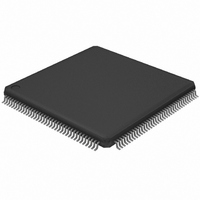
LPC2294HBD144,551 NXP Semiconductors, LPC2294HBD144,551 Datasheet - Page 32

LPC2294HBD144,551
Manufacturer Part Number
LPC2294HBD144,551
Description
IC ARM7 MCU FLASH 256K 144-LQFP
Manufacturer
NXP Semiconductors
Series
LPC2200r
Datasheet
1.LPC2292FBD144015.pdf
(53 pages)
Specifications of LPC2294HBD144,551
Core Processor
ARM7
Core Size
16/32-Bit
Speed
60MHz
Connectivity
CAN, EBI/EMI, I²C, Microwire, SPI, SSI, SSP, UART/USART
Peripherals
POR, PWM, WDT
Number Of I /o
112
Program Memory Size
256KB (256K x 8)
Program Memory Type
FLASH
Ram Size
16K x 8
Voltage - Supply (vcc/vdd)
1.65 V ~ 3.6 V
Data Converters
A/D 8x10b
Oscillator Type
Internal
Operating Temperature
-40°C ~ 125°C
Package / Case
144-LQFP
For Use With
OM10091 - KIT DEV PHYCORE-ARM7/LPC2220568-1757 - BOARD EVAL FOR LPC220X ARM MCU
Lead Free Status / RoHS Status
Lead free / RoHS Compliant
Eeprom Size
-
Other names
568-2383
935278705551
LPC2294HBD144-S
935278705551
LPC2294HBD144-S
Available stocks
Company
Part Number
Manufacturer
Quantity
Price
Company:
Part Number:
LPC2294HBD144,551
Manufacturer:
NXP Semiconductors
Quantity:
10 000
NXP Semiconductors
Table 7.
T
[1]
[2]
[3]
[4]
[5]
[6]
[7]
[8]
[9]
[10] Applies to P1[25:16].
[11] See the LPC2119/2129/2194/2292/2294 User Manual .
[12] To V
Table 8.
V
[1]
[2]
[3]
[4]
[5]
[6]
[7]
LPC2292_2294_7
Product data sheet
Symbol
Oscillator pins
V
V
Symbol
V
C
E
E
E
E
E
amb
DDA
i(XTAL1)
o(XTAL2)
IA
D
L(adj)
O
G
T
ia
Typical ratings are not guaranteed. The values listed are at room temperature (+25 C), nominal supply voltages.
Internal rail.
External rail.
Including voltage on outputs in 3-state mode.
V
3-state outputs go into 3-state mode when V
Accounts for 100 mV voltage drop in all supply lines.
Allowed as long as the current limit does not exceed the maximum current allowed by the device.
Minimum condition for V
Conditions: V
The ADC is monotonic, there are no missing codes.
The differential linearity error (E
The integral non-linearity (E
appropriate adjustment of gain and offset errors. See
The offset error (E
ideal curve. See
The gain error (E
error, and the straight line which fits the ideal transfer curve. See
The absolute voltage error (E
non-calibrated ADC and the ideal transfer curve. See
= 40 C to +125 C, unless otherwise specified.
= 2.5 V to 3.6 V; T
DD(3V3)
SS
.
Parameter
input voltage on pin XTAL1
output voltage on pin
XTAL2
Static characteristics
ADC static characteristics
supply voltages must be present.
Parameter
analog input voltage
analog input
capacitance
differential linearity
error
integral non-linearity
offset error
gain error
absolute error
SSA
Figure
G
= 0 V, V
O
) is the relative difference in percent between the straight line fitting the actual transfer curve after removing offset
) is the absolute difference between the straight line which fits the actual curve and the straight line which fits the
amb
5.
I
= 4.5 V, maximum condition for V
DDA
= 40 C to +125 C unless otherwise specified. ADC frequency 4.5 MHz.
L(adj)
T
= 3.3 V.
) is the maximum difference between the center of the steps of the actual transfer curve of the
D
) is the peak difference between the center of the steps of the actual and the ideal transfer curve after
) is the difference between the actual step width and the ideal step width. See
…continued
Conditions
Conditions
DD(3V3)
Rev. 7 — 4 December 2008
16/32-bit ARM microcontrollers with external memory interface
is grounded.
Figure
Figure
I
= 5.5 V.
5.
5.
Figure
5.
[1][2][3]
[1][4]
[1][5]
[1][6]
[1][7]
Min
0
-
-
-
-
-
-
Min
0
0
LPC2292/LPC2294
Typ
-
-
-
-
-
-
-
Typ
-
-
[1]
Max
V
1
Figure
© NXP B.V. 2008. All rights reserved.
1
2
3
0.5
4
DDA
Max
1.8
1.8
5.
Unit
V
pF
LSB
LSB
LSB
%
LSB
32 of 53
Unit
V
V


