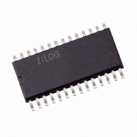
Z8F0223SJ005EG Zilog, Z8F0223SJ005EG Datasheet - Page 146

Z8F0223SJ005EG
Manufacturer Part Number
Z8F0223SJ005EG
Description
IC ENCORE MCU FLASH 2K 28SOIC
Manufacturer
Zilog
Series
Encore!® XP®r
Datasheet
1.Z8F0223SB005SG.pdf
(247 pages)
Specifications of Z8F0223SJ005EG
Core Processor
Z8
Core Size
8-Bit
Speed
5MHz
Connectivity
IrDA, UART/USART
Peripherals
Brown-out Detect/Reset, LED, POR, PWM, WDT
Number Of I /o
22
Program Memory Size
2KB (2K x 8)
Program Memory Type
FLASH
Ram Size
512 x 8
Voltage - Supply (vcc/vdd)
2.7 V ~ 3.6 V
Data Converters
A/D 8x10b
Oscillator Type
Internal
Operating Temperature
-40°C ~ 105°C
Package / Case
28-SOIC (7.5mm Width)
Lead Free Status / RoHS Status
Lead free / RoHS Compliant
Eeprom Size
-
Other names
269-4082
Z8F0223SJ005EG
Z8F0223SJ005EG
- Current page: 146 of 247
- Download datasheet (4Mb)
PS024314-0308
Caution:
Flash Controller Bypass
Flash Controller Behavior in DEBUG Mode
value
Controller executes the Mass Erase operation, the eZ8 CPU idles but the system clock and
on-chip peripherals continue to operate. Using the On-Chip Debugger, poll the Flash
Status register to determine when the Mass Erase operation is complete. When the Mass
Erase is complete, the Flash Controller returns to its locked state.
The Flash Controller can be bypassed and the control signals for the Flash memory
brought out to the GPIO pins. Bypassing the Flash Controller allows faster Row Program-
ming algorithms by controlling the Flash programming signals directly.
Row programing is recommended for gang programming applications and large volume
customers who do not require in-circuit initial programming of the Flash memory. Page
Erase operations are also supported when the Flash Controller is bypassed.
For more information on bypassing the Flash Controller, refer to Third-Party Flash Pro-
gramming Support for Z8 Encore! (AN0117) available for download at www.zilog.com.
The following changes in behavior of the Flash Controller occur when the Flash
Controller is accessed using the On-Chip Debugger:
•
•
•
•
•
•
•
For security reasons, Flash controller allows only a single page to be opened for write/
erase. When writing multiple Flash pages, the Flash controller must go through the un-
lock sequence again to select another page.
The Flash Write Protect option bit is ignored
The Flash Sector Protect register is ignored for programming and erase operations
Programming operations are not limited to the page selected in the Page Select
register
Bits in the Flash Sector Protect register can be written to one or zero
The second write of the Page Select register to unlock the Flash Controller is not
necessary
The Page Select register can be written when the Flash Controller is unlocked
The Mass Erase command is enabled through the Flash Control register
63H
to the Flash Control register initiates the Mass Erase operation. While the Flash
Z8 Encore! XP
Product Specification
®
F0823 Series
Flash Memory
136
Related parts for Z8F0223SJ005EG
Image
Part Number
Description
Manufacturer
Datasheet
Request
R

Part Number:
Description:
Communication Controllers, ZILOG INTELLIGENT PERIPHERAL CONTROLLER (ZIP)
Manufacturer:
Zilog, Inc.
Datasheet:

Part Number:
Description:
KIT DEV FOR Z8 ENCORE 16K TO 64K
Manufacturer:
Zilog
Datasheet:

Part Number:
Description:
KIT DEV Z8 ENCORE XP 28-PIN
Manufacturer:
Zilog
Datasheet:

Part Number:
Description:
DEV KIT FOR Z8 ENCORE 8K/4K
Manufacturer:
Zilog
Datasheet:

Part Number:
Description:
KIT DEV Z8 ENCORE XP 28-PIN
Manufacturer:
Zilog
Datasheet:

Part Number:
Description:
DEV KIT FOR Z8 ENCORE 4K TO 8K
Manufacturer:
Zilog
Datasheet:

Part Number:
Description:
CMOS Z8 microcontroller. ROM 16 Kbytes, RAM 256 bytes, speed 16 MHz, 32 lines I/O, 3.0V to 5.5V
Manufacturer:
Zilog, Inc.
Datasheet:

Part Number:
Description:
Low-cost microcontroller. 512 bytes ROM, 61 bytes RAM, 8 MHz
Manufacturer:
Zilog, Inc.
Datasheet:

Part Number:
Description:
Z8 4K OTP Microcontroller
Manufacturer:
Zilog, Inc.
Datasheet:

Part Number:
Description:
CMOS SUPER8 ROMLESS MCU
Manufacturer:
Zilog, Inc.
Datasheet:

Part Number:
Description:
SL1866 CMOSZ8 OTP Microcontroller
Manufacturer:
Zilog, Inc.
Datasheet:

Part Number:
Description:
SL1866 CMOSZ8 OTP Microcontroller
Manufacturer:
Zilog, Inc.
Datasheet:

Part Number:
Description:
OTP (KB) = 1, RAM = 125, Speed = 12, I/O = 14, 8-bit Timers = 2, Comm Interfaces Other Features = Por, LV Protect, Voltage = 4.5-5.5V
Manufacturer:
Zilog, Inc.
Datasheet:

Part Number:
Description:
Manufacturer:
Zilog, Inc.
Datasheet:


