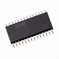
Z8F0223SJ005EG Zilog, Z8F0223SJ005EG Datasheet - Page 47

Z8F0223SJ005EG
Manufacturer Part Number
Z8F0223SJ005EG
Description
IC ENCORE MCU FLASH 2K 28SOIC
Manufacturer
Zilog
Series
Encore!® XP®r
Datasheet
1.Z8F0223SB005SG.pdf
(247 pages)
Specifications of Z8F0223SJ005EG
Core Processor
Z8
Core Size
8-Bit
Speed
5MHz
Connectivity
IrDA, UART/USART
Peripherals
Brown-out Detect/Reset, LED, POR, PWM, WDT
Number Of I /o
22
Program Memory Size
2KB (2K x 8)
Program Memory Type
FLASH
Ram Size
512 x 8
Voltage - Supply (vcc/vdd)
2.7 V ~ 3.6 V
Data Converters
A/D 8x10b
Oscillator Type
Internal
Operating Temperature
-40°C ~ 105°C
Package / Case
28-SOIC (7.5mm Width)
Lead Free Status / RoHS Status
Lead free / RoHS Compliant
Eeprom Size
-
Other names
269-4082
Z8F0223SJ005EG
Z8F0223SJ005EG
- Current page: 47 of 247
- Download datasheet (4Mb)
Direct LED Drive
Shared Reset Pin
Shared Debug Pin
PS024314-0308
Caution:
Caution:
PA0 and PA6 contain two different timer functions, a timer input and a complementary
timer output. Both of these functions require the same GPIO configuration, the selection
between the two is based on the timer mode. For more details, see
The Port C pins provide a current sinked output capable of driving an LED without
requiring an external resistor. The output sinks current at programmable levels of 3 mA,
7 mA, 13 mA, and 20 mA. This mode is enabled through the Alternate Function
sub-register AFS1 and is programmable through the LED control registers. The LED
Drive Enable (LEDEN) register turns on the drivers. The LED Drive Level (LEDLVLH
and LEDLVLL) registers select the sink current.
For correct function, the LED anode must be connected to V
GPIO pin. Using all Port C pins in LED drive mode with maximum current can result in
excessive total current. For the maximum total current for the applicable package, see
Electrical Characteristics
On the 8-pin product versions, the reset pin is shared with PA2, but the pin is not
limited to output-only when in GPIO mode.
On the 8-pin version of this device only, the Debug pin shares function with the PA0 GPIO
pin. This pin performs as a general purpose input pin on power-up, but the debug logic
monitors this pin during the reset sequence to determine if the unlock sequence occurs. If
the unlock sequence is present, the debug function is unlocked and the pin no longer func-
For pin with multiple alternate functions, it is recommended to write to the
AFS1 and AFS2 sub-registers before enabling the alternate function via
the AF sub-register. This prevents spurious transitions through unwanted
alternate function modes.
If PA2 on the 8-pin product is reconfigured as an input, take care that no
external stimulus drives the pin Low during any reset sequence. Since PA2
returns to its RESET alternate function during system resets, driving it Low
holds the chip in a reset state until the pin is released.
on page 193.
Z8 Encore! XP
DD
General-Purpose Input/Output
and the cathode to the
Product Specification
Timers
®
on page 67.
F0823 Series
37
Related parts for Z8F0223SJ005EG
Image
Part Number
Description
Manufacturer
Datasheet
Request
R

Part Number:
Description:
Communication Controllers, ZILOG INTELLIGENT PERIPHERAL CONTROLLER (ZIP)
Manufacturer:
Zilog, Inc.
Datasheet:

Part Number:
Description:
KIT DEV FOR Z8 ENCORE 16K TO 64K
Manufacturer:
Zilog
Datasheet:

Part Number:
Description:
KIT DEV Z8 ENCORE XP 28-PIN
Manufacturer:
Zilog
Datasheet:

Part Number:
Description:
DEV KIT FOR Z8 ENCORE 8K/4K
Manufacturer:
Zilog
Datasheet:

Part Number:
Description:
KIT DEV Z8 ENCORE XP 28-PIN
Manufacturer:
Zilog
Datasheet:

Part Number:
Description:
DEV KIT FOR Z8 ENCORE 4K TO 8K
Manufacturer:
Zilog
Datasheet:

Part Number:
Description:
CMOS Z8 microcontroller. ROM 16 Kbytes, RAM 256 bytes, speed 16 MHz, 32 lines I/O, 3.0V to 5.5V
Manufacturer:
Zilog, Inc.
Datasheet:

Part Number:
Description:
Low-cost microcontroller. 512 bytes ROM, 61 bytes RAM, 8 MHz
Manufacturer:
Zilog, Inc.
Datasheet:

Part Number:
Description:
Z8 4K OTP Microcontroller
Manufacturer:
Zilog, Inc.
Datasheet:

Part Number:
Description:
CMOS SUPER8 ROMLESS MCU
Manufacturer:
Zilog, Inc.
Datasheet:

Part Number:
Description:
SL1866 CMOSZ8 OTP Microcontroller
Manufacturer:
Zilog, Inc.
Datasheet:

Part Number:
Description:
SL1866 CMOSZ8 OTP Microcontroller
Manufacturer:
Zilog, Inc.
Datasheet:

Part Number:
Description:
OTP (KB) = 1, RAM = 125, Speed = 12, I/O = 14, 8-bit Timers = 2, Comm Interfaces Other Features = Por, LV Protect, Voltage = 4.5-5.5V
Manufacturer:
Zilog, Inc.
Datasheet:

Part Number:
Description:
Manufacturer:
Zilog, Inc.
Datasheet:


