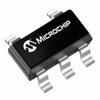
MCP6001UT-I/OT Microchip Technology, MCP6001UT-I/OT Datasheet - Page 14

MCP6001UT-I/OT
Manufacturer Part Number
MCP6001UT-I/OT
Description
IC OPAMP SGL 1.8V R-R I/O SOT235
Manufacturer
Microchip Technology
Specifications of MCP6001UT-I/OT
Slew Rate
0.6 V/µs
Package / Case
SOT-23-5, SC-74A, SOT-25
Amplifier Type
General Purpose
Number Of Circuits
1
Output Type
Rail-to-Rail
Gain Bandwidth Product
1MHz
Current - Input Bias
1pA
Voltage - Input Offset
4500µV
Current - Supply
100µA
Current - Output / Channel
23mA
Voltage - Supply, Single/dual (±)
1.8 V ~ 6 V
Operating Temperature
-40°C ~ 85°C
Mounting Type
Surface Mount
Number Of Channels
1
Common Mode Rejection Ratio (min)
60 dB
Input Offset Voltage
4.5 mV
Input Bias Current (max)
19 pA
Operating Supply Voltage
3 V, 5 V
Maximum Operating Temperature
+ 85 C
Minimum Operating Temperature
- 40 C
Mounting Style
SMD/SMT
Shutdown
No
Supply Voltage (max)
6 V
Supply Voltage (min)
1.8 V
Technology
CMOS
Voltage Gain Db
112 dB
Lead Free Status / RoHS Status
Lead free / RoHS Compliant
For Use With
MCP6SX2DM-PCTLPD - BOARD DAUGHTER PICTAIL MCP6SX2
-3db Bandwidth
-
Lead Free Status / Rohs Status
Lead free / RoHS Compliant
Other names
MCP6001UT-I/OT
MCP6001UT-I/OTRTR
MCP6001UT-I/OTRTR
MCP6001UT-I/OTTR
MCP6001UT-I/OTRTR
MCP6001UT-I/OTRTR
MCP6001UT-I/OTTR
Available stocks
Company
Part Number
Manufacturer
Quantity
Price
Company:
Part Number:
MCP6001UT-I/OT
Manufacturer:
TI
Quantity:
3 000
Part Number:
MCP6001UT-I/OT
Manufacturer:
MICROCH1P
Quantity:
20 000
MCP6001/1R/1U/2/4
4.3
Driving large capacitive loads can cause stability
problems for voltage feedback op amps. As the load
capacitance increases, the feedback loop’s phase
margin decreases and the closed-loop bandwidth is
reduced. This produces gain peaking in the frequency
response, with overshoot and ringing in the step
response. While a unity-gain buffer (G = +1) is the most
sensitive to capacitive loads, all gains show the same
general behavior.
When driving large capacitive loads with these op
amps (e.g., > 100 pF when G = +1), a small series
resistor at the output (R
feedback loop’s phase margin (stability) by making the
output load resistive at higher frequencies. The
bandwidth will be generally lower than the bandwidth
with no capacitance load.
FIGURE 4-3:
stabilizes large capacitive loads.
Figure 4-4
different capacitive loads and gains. The x-axis is the
normalized load capacitance (C
circuit's noise gain. For non-inverting gains, G
Signal Gain are equal. For inverting gains, G
1+|Signal Gain| (e.g., -1 V/V gives G
FIGURE 4-4:
for Capacitive Loads.
After selecting R
resulting frequency response peaking and step
response overshoot. Modify R
response is reasonable. Bench evaluation and
simulations with the MCP6001/1R/1U/2/4 SPICE
macro model are very helpful.
DS21733J-page 14
V
IN
1000
100
10
1.E-11
10p
Capacitive Loads
V
R
DD
G
G
L
gives recommended R
= 100 k
N
N
–
MCP600X
+
Normalized Load Capacitance; C
= 5.0V
= 1
≥ 2
ISO
1.E-10
for your circuit, double-check the
100p
Output resistor, R
Recommended R
ISO
in
Figure
R
L
ISO
ISO
/G
1.E-09
C
N
1n
’s value until the
), where G
N
L
4-3) improves the
ISO
= +2 V/V).
L
/G
ISO
ISO
values for
N
(F)
N
V
values
1.E-08
and the
N
10n
OUT
is the
N
is
4.4
With this family of operational amplifiers, the power
supply pin (V
bypass capacitor (i.e., 0.01 µF to 0.1 µF) within 2 mm
for good high-frequency performance. It also needs a
bulk capacitor (i.e., 1 µF or larger) within 100 mm to
provide large, slow currents. This bulk capacitor can be
shared with nearby analog parts.
4.5
An unused op amp in a quad package (MCP6004)
should be configured as shown in
circuits prevent the output from toggling and causing
crosstalk. Circuits A sets the op amp at its minimum
noise gain. The resistor divider produces any desired
reference voltage within the output voltage range of the
op amp; the op amp buffers that reference voltage.
Circuit B uses the minimum number of components
and operates as a comparator, but it may draw more
current.
FIGURE 4-5:
4.6
In applications where low input bias current is critical,
Printed Circuit Board (PCB) surface leakage effects
need to be considered. Surface leakage is caused by
humidity, dust or other contamination on the board.
Under low humidity conditions, a typical resistance
between nearby traces is 10
cause 5 pA of current to flow; which is greater than the
MCP6001/1R/1U/2/4 family’s bias current at 25°C (typ-
ically 1 pA).
The easiest way to reduce surface leakage is to use a
guard ring around sensitive pins (or traces). The guard
ring is biased at the same voltage as the sensitive pin.
An example of this type of layout is shown in
Figure
V
DD
¼ MCP6004 (A)
V
REF
R
R
4-6.
1
2
Supply Bypass
Unused Op Amps
PCB Surface Leakage
=
V
DD
DD
V
DD
for single-supply) should have a local
•
------------------
R
1
R
+
Unused Op Amps.
2
R
© 2009 Microchip Technology Inc.
V
2
REF
12
Ω. A 5V difference would
Figure
¼ MCP6004 (B)
V
4-5. These
DD


