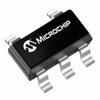
MCP6001UT-I/OT Microchip Technology, MCP6001UT-I/OT Datasheet - Page 16

MCP6001UT-I/OT
Manufacturer Part Number
MCP6001UT-I/OT
Description
IC OPAMP SGL 1.8V R-R I/O SOT235
Manufacturer
Microchip Technology
Specifications of MCP6001UT-I/OT
Slew Rate
0.6 V/µs
Package / Case
SOT-23-5, SC-74A, SOT-25
Amplifier Type
General Purpose
Number Of Circuits
1
Output Type
Rail-to-Rail
Gain Bandwidth Product
1MHz
Current - Input Bias
1pA
Voltage - Input Offset
4500µV
Current - Supply
100µA
Current - Output / Channel
23mA
Voltage - Supply, Single/dual (±)
1.8 V ~ 6 V
Operating Temperature
-40°C ~ 85°C
Mounting Type
Surface Mount
Number Of Channels
1
Common Mode Rejection Ratio (min)
60 dB
Input Offset Voltage
4.5 mV
Input Bias Current (max)
19 pA
Operating Supply Voltage
3 V, 5 V
Maximum Operating Temperature
+ 85 C
Minimum Operating Temperature
- 40 C
Mounting Style
SMD/SMT
Shutdown
No
Supply Voltage (max)
6 V
Supply Voltage (min)
1.8 V
Technology
CMOS
Voltage Gain Db
112 dB
Lead Free Status / RoHS Status
Lead free / RoHS Compliant
For Use With
MCP6SX2DM-PCTLPD - BOARD DAUGHTER PICTAIL MCP6SX2
-3db Bandwidth
-
Lead Free Status / Rohs Status
Lead free / RoHS Compliant
Other names
MCP6001UT-I/OT
MCP6001UT-I/OTRTR
MCP6001UT-I/OTRTR
MCP6001UT-I/OTTR
MCP6001UT-I/OTRTR
MCP6001UT-I/OTRTR
MCP6001UT-I/OTTR
Available stocks
Company
Part Number
Manufacturer
Quantity
Price
Company:
Part Number:
MCP6001UT-I/OT
Manufacturer:
TI
Quantity:
3 000
Part Number:
MCP6001UT-I/OT
Manufacturer:
MICROCH1P
Quantity:
20 000
MCP6001/1R/1U/2/4
4.7.3
The MCP6001/2/4 op amp has a high input impedance,
rail-to-rail input/output and low input bias current, which
makes this device suitable for peak detector
applications.
with clear and sample switches. The peak-detection
cycle uses a clock (CLK), as shown in
At the rising edge of CLK, Sample Switch closes to
begin sampling. The peak voltage stored on C
sampled to C
the end of the sample time (falling edge of Sample
Signal), Clear Signal goes high and closes the Clear
Switch. When the Clear Switch closes, C
through R
the clear time (falling edge of Clear Signal), op amp A
begins to store the peak value of V
defined by t
In order to define t
determine the capacitor charging and discharging
period. The capacitor charging time is limited by the
amplifier source current, while the discharging time (
is defined using R
the input signal is sampled on C
the input voltage change frequency.
The op amp output current limit, and the size of the
storage capacitors (both C
slewing limitations as the input voltage (V
Current through a capacitor is dependent on the size of
the capacitor and the rate of voltage change. From this
relationship, the rate of voltage change or the slew rate
can be determined. For example, with an op amp short
circuit current of I
C
FIGURE 4-9:
DS21733J-page 16
V
1
IN
= 0.1 µF, then:
MCP6002
+
–
1
1/2
DETECT
PEAK DETECTOR
for a time defined by t
Figure 4-9
2
Op Amp A
for a sample time defined by t
1
SC
.
SAMP
(
τ
= 25 mA and a load capacitor of
D
= R
Peak Detector with Clear and Sample CMOS Analog Switches.
1
shows a peak detector circuit
and t
1
C
1
1
R
). t
CLEAR
ISO
and C
DETECT
1
and is dependent on
CLEAR
Switch
Clear
V
IN
, it is necessary to
C1
2
on C
Figure
), could create
C
is the time that
. At the end of
1
IN
1
Sample Signal
) increases.
1
discharges
Clear Signal
for a time
4-9.
SAMP
R
1
1
. At
CLK
τ
is
)
MCP6002
+
–
1/2
Op Amp B
t
SAMP
t
CLEAR
EQUATION 4-1:
This voltage rate of change is less than the MCP6001/2/4
slew rate of 0.6 V/µs. When the input voltage swings
below the voltage across C
biased. This opens the feedback loop and rails the
amplifier. When the input voltage increases, the amplifier
recovers at its slew rate. Based on the rate of voltage
change shown in the above equation, it takes an
extended period of time to charge a 0.1 µF capacitor. The
capacitors need to be selected so that the circuit is not
limited by the amplifier slew rate. Therefore, the
capacitors should be less than 40 µF and a stabilizing
resistor (R
Section 4.3 “Capacitive Loads”).
t
DETECT
Sample
Switch
ISO
) needs to be properly selected. (Refer to
R
dV
------------ -
ISO
dt
dV
------------ -
C1
dt
C1
I
SC
V
=
© 2009 Microchip Technology Inc.
C2
=
=
250mV μs
=
C
I
------- -
-------------- -
0.1μF
C
25mA
SC
C
2
1
1
, D
1
dV
------------ -
dt
⁄
MCP6001
1
+
–
C1
becomes reverse-
Op Amp C
V
OUT


