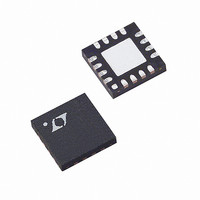
LTC6404IUD-2#PBF Linear Technology, LTC6404IUD-2#PBF Datasheet

LTC6404IUD-2#PBF
Specifications of LTC6404IUD-2#PBF
Available stocks
Related parts for LTC6404IUD-2#PBF
LTC6404IUD-2#PBF Summary of contents
Page 1
... The LTC6404-2 is available in a compact 3mm × 3mm 16-pin leadless QFN package and operates over a –40°C to 125°C temperature range. L, LT, LTC and LTM are registered trademarks of Linear Technology Corporation. All other trademarks are the property of their respective owners. 1V P-P ...
Page 2
... ORDER INFORMATION LEAD FREE FINISH TAPE AND REEL LTC6404CUD-2#PBF LTC6404CUD-2#TRPBF LTC6404IUD-2#PBF LTC6404IUD-2#TRPBF LTC6404HUD-2#PBF LTC6404HUD-2#TRPBF Consult LTC Marketing for parts specifi ed with wider operating temperature ranges. *The temperature grade is identifi label on the shipping container. Consult LTC Marketing for information on non-standard lead based fi nish parts. ...
Page 3
LTC6404-2 DC ELECTRICAL CHARACTERISTICS over the full operating temperature range, otherwise specifi cations are OPEN 100Ω 200Ω, R SHDN – )/ defi ...
Page 4
LTC6404-2 LTC6404-2 DC ELECTRICAL CHARACTERISTICS over the full operating temperature range, otherwise specifi cations are OPEN 100Ω 200Ω, R SHDN – )/ ...
Page 5
LTC6404-2 ELECTRICAL CHARACTERISTICS Note 1: Stresses beyond those listed under Absolute Maximum Ratings may cause permanent damage to the device. Exposure to any Absolute Maximum Rating condition for extended periods may affect device reliability and lifetime. + – Note 2: ...
Page 6
LTC6404-2 TYPICAL PERFORMANCE CHARACTERISTICS Active Supply Current vs Temperature MID-SUPPLY CM OCM 32 2. 27.5 25 –75 –50 – ...
Page 7
TYPICAL PERFORMANCE CHARACTERISTICS Small Signal Frequency Response vs Gain Setting Resistor Values 100Ω 200Ω 200Ω 400Ω 499Ω 1kΩ ...
Page 8
LTC6404-2 TYPICAL PERFORMANCE CHARACTERISTICS Distortion vs Output Amplitude – MID-SUPPLY CM OCM – 100Ω 200Ω SINGLE-ENDED INPUT IN – 10MHz IN –70 ...
Page 9
PIN FUNCTIONS pin has an input resistance of approximately 14k to a mid-supply potential. The V pin should be bypassed OCM with a high quality ceramic bypass capacitor of at least 0.01μF , (with symmetrical split supplies, connect directly to ...
Page 10
LTC6404-2 APPLICATIONS INFORMATION + V INP – SHDN V SHDN 0.1μ – OCM 0.01μ INM – 0.01μF MINI-CIRCUITS TCM4-19 50Ω V SHDN + + V ...
Page 11
APPLICATIONS INFORMATION Functional Description The LTC6404 small outline, wide band, low noise, and low distortion fully-differential amplifi er with accurate output phase balancing. The LTC6404-2 is optimized to drive low voltage, single-supply, differential input analog- to-digital converters (ADCs). ...
Page 12
LTC6404-2 APPLICATIONS INFORMATION appear as open collectors with a non-linear capacitor in parallel and steering diodes to either supply. Because of the non-linear capacitance, the outputs still have the ability to sink and source small amounts of transient current if ...
Page 13
APPLICATIONS INFORMATION When the feedback ratios mismatch (Δβ), common mode to differential conversion occurs. Setting the differential input to zero (V gree of common mode to differential conversion is given by the equation – V – V ...
Page 14
LTC6404-2 APPLICATIONS INFORMATION R INM CHOSEN SO THAT INM S R2 CHOSEN TO BALANCE Figure ...
Page 15
APPLICATIONS INFORMATION which incorporate an internal lowpass fi lter network with a –3dB bandwidth of 88.5MHz (Figure 6). These pins each have a DC output impedance of 50Ω. In- – ternal capacitances are 12pF each fi ltered ...
Page 16
LTC6404-2 APPLICATIONS INFORMATION Noise Considerations The LTC6404-2’s input referred voltage noise is on the order of 1.5nV/√Hz. Its input referred current noise is on the order of 3pA/√Hz. In addition to the noise generated by the amplifi er, the feedback ...
Page 17
APPLICATIONS INFORMATION 100 TOTAL (AMPLIFIER AND FEEDBACK NETWORK) OUTPUT NOISE 10 FEEDBACK RESISTOR NETWORK NOISE ALONE 1 0.1 10 100 • R (Ω Figure 10. LTC6404-2 Output Spot Noise vs Spot Noise Contributed by ...
Page 18
LTC6404-2 APPLICATIONS INFORMATION make the apparent voltage offset of the amplifi er appear worse than specifi ed. In general, the apparent input referred offset induced by feedback factor mismatch is given by the equation: V ≈ (V – V OSDIFF(APPARENT) ...
Page 19
... ON THE TOP AND BOTTOM OF PACKAGE Information furnished by Linear Technology Corporation is believed to be accurate and reliable. However, no responsibility is assumed for its use. Linear Technology Corporation makes no representa- tion that the interconnection of its circuits as described herein will not infringe on existing patent rights. UD Package 16-Lead Plastic QFN (3mm × ...
Page 20
... S/N with 3V Supply, SO-8 Package 76dB S/N with 3V Supply, SO-8 Package www.linear.com ● , 1MHz: –94dBc, 13mA, Low Noise: 3nV/√Hz P-P = 200Ω 105mA at 25°C IN S(MAX) = 200Ω 62mA at 25°C IN S(MAX) =18mA S LT 0208 • PRINTED IN USA © LINEAR TECHNOLOGY CORPORATION 2008 64042f ...


