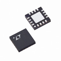
LTC6404IUD-2#PBF Linear Technology, LTC6404IUD-2#PBF Datasheet - Page 11

LTC6404IUD-2#PBF
Manufacturer Part Number
LTC6404IUD-2#PBF
Description
IC AMP/DRIVER DIFF 16-QFN
Manufacturer
Linear Technology
Type
ADC Driverr
Specifications of LTC6404IUD-2#PBF
Applications
Data Acquisition
Mounting Type
Surface Mount
Package / Case
16-WQFN Exposed Pad
Current - Supply
30.4mA
Operating Temperature
-40°C ~ 85°C
Output Type
Differential, Rail-to-Rail
Number Of Circuits
1
Current - Output / Channel
85mA
Amplifier Type
Differential
Voltage - Supply, Single/dual (±)
2.7 V ~ 5.5 V, ±1.35 V ~ 2.75 V
-3db Bandwidth
600MHz
Slew Rate
700 V/µs
Gain Bandwidth Product
900MHz
Current - Input Bias
23µA
Voltage - Input Offset
500µV
Number Of Channels
1
Number Of Elements
1
Power Supply Requirement
Single
Common Mode Rejection Ratio
60dB
Voltage Gain Db
90dB
Unity Gain Bandwidth Product (typ)
900MHz
Input Resistance
1@3V@-40C TO 85CMohm
Single Supply Voltage (typ)
3/5V
Dual Supply Voltage (typ)
Not RequiredV
Power Supply Rejection Ratio
60dB
Rail/rail I/o Type
Rail to Rail Output
Single Supply Voltage (min)
2.7V
Single Supply Voltage (max)
5.25V
Dual Supply Voltage (min)
Not RequiredV
Dual Supply Voltage (max)
Not RequiredV
Operating Temp Range
-40C to 85C
Operating Temperature Classification
Industrial
Mounting
Surface Mount
Pin Count
16
Package Type
QFN EP
No. Of Amplifiers
1
Input Offset Voltage
2mV
Gain Db Max
2dB
Bandwidth
900MHz
Supply Voltage Range
2.7V To 5.25V
Supply Current
30.4mA
Amplifier Case Style
QFN
Rohs Compliant
Yes
Lead Free Status / RoHS Status
Lead free / RoHS Compliant
Available stocks
Company
Part Number
Manufacturer
Quantity
Price
APPLICATIONS INFORMATION
Functional Description
The LTC6404-2 is a small outline, wide band, low noise,
and low distortion fully-differential amplifi er with accurate
output phase balancing. The LTC6404-2 is optimized to
drive low voltage, single-supply, differential input analog-
to-digital converters (ADCs). The LTC6404-2’s output is
capable of swinging rail-to-rail on supplies as low as 2.7V,
which makes the amplifi er ideal for converting ground
referenced, single-ended signals into DC level shifted
differential signals in preparation for driving low voltage,
single-supply, differential input ADCs. Unlike traditional
op amps which have a single output, the LTC6404-2 has
two outputs to process signals differentially. This allows
for two times the signal swing in low voltage systems
when compared to single-ended output amplifi ers. The
balanced differential nature of the amplifi er also provides
even-order harmonic distortion cancellation, and less
susceptibility to common mode noise (i.e. power supply
noise). The LTC6404-2 can be used as a single ended input
to differential output amplifi er, or as a differential input to
differential output amplifi er.
The LTC6404-2’s output common mode voltage, defi ned
as the average of the two output voltages, is independent
of the input common mode voltage, and is adjusted by
applying a voltage on the V
there is an internal resistive voltage divider that develops
a potential halfway between the V
this pin is not hard tied to a low impedance ground plane,
it is recommended that a high quality ceramic cap is used
to bypass the V
(See Layout Considerations). The LTC6404-2’s internal
common mode feedback path forces accurate output
phase balancing to reduce even order harmonics, and
centers each individual output about the potential set by
the V
The outputs (OUT
pable of swinging rail-to-rail. They can source or sink up
to approximately 65mA of current.
V
OUTCM
OCM
pin.
= V
OCM
OCM
+
=
pin to a low impedance ground plane
and OUT
V
OUT
+
OCM
+ V
2
–
) of the LTC6404-2 are ca-
pin. If the pin is left open,
OUT
+
and V
–
–
pins. Whenever
Additional outputs (OUTF
provide fi ltered versions of the OUT
on-chip single pole RC passive fi lter bandlimits the fi ltered
outputs to a –3dB frequency of 88.5MHz. The user has a
choice of using the unfi ltered outputs, the fi ltered outputs,
or modifying the fi ltered outputs to adjust the frequency
response by adding additional components.
In applications where the full bandwidth of the LTC6404-2
is desired, the unfi ltered outputs (OUT
be used. The unfi ltered outputs OUT
designed to drive 10pF to ground (or 5pF differentially).
Capacitances greater than 10pF will produce excess peak-
ing, and can be mitigated by placing at least 25Ω in series
with the output.
Input Pin Protection
The LTC6404-2’s input stage is protected against differ-
ential input voltages which exceed 1.4V by two pairs of
series diodes connected in opposite directions between
IN
have steering diodes to either power supply. If the input
pair is over-driven, the current should be limited to 10mA
to prevent damage to the IC. The LTC6404-2 also has
steering diodes to either power supply on the V
SHDN pins (Pins 4 and 1) and if forced to voltages which
exceed either supply, they too, should be current limited
to 10mA.
SHDN Pin
If the SHDN pin (Pin 1) is pulled 2.1V below the positive
supply, circuitry is activated which powers down the
LTC6404-2. The pin will have the Thevenin equivalent
impedance of approximately 66kΩ to V
left unconnected, an internal pull-up resistor of 150k will
keep the part in normal active operation. Care should
be taken to control leakage currents at this pin to under
1μA to prevent inadvertently putting the LTC6404-2 into
shutdown. In shutdown, all biasing current sources are
shut off, and the output pins, OUT
+
and IN
–
(Pins 6 and 15). In addition, the input pins
+
and OUTF
+
+
and OUT
LTC6404-2
and OUT
–
+
) are available that
and OUT
+
+
and OUT
. If the pin is
–
outputs. An
–
, will each
–
OCM
) should
11
–
, and
64042f
are


