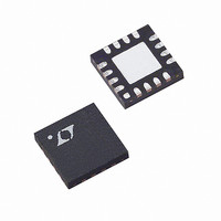
LTC6404IUD-2#PBF Linear Technology, LTC6404IUD-2#PBF Datasheet - Page 4

LTC6404IUD-2#PBF
Manufacturer Part Number
LTC6404IUD-2#PBF
Description
IC AMP/DRIVER DIFF 16-QFN
Manufacturer
Linear Technology
Type
ADC Driverr
Specifications of LTC6404IUD-2#PBF
Applications
Data Acquisition
Mounting Type
Surface Mount
Package / Case
16-WQFN Exposed Pad
Current - Supply
30.4mA
Operating Temperature
-40°C ~ 85°C
Output Type
Differential, Rail-to-Rail
Number Of Circuits
1
Current - Output / Channel
85mA
Amplifier Type
Differential
Voltage - Supply, Single/dual (±)
2.7 V ~ 5.5 V, ±1.35 V ~ 2.75 V
-3db Bandwidth
600MHz
Slew Rate
700 V/µs
Gain Bandwidth Product
900MHz
Current - Input Bias
23µA
Voltage - Input Offset
500µV
Number Of Channels
1
Number Of Elements
1
Power Supply Requirement
Single
Common Mode Rejection Ratio
60dB
Voltage Gain Db
90dB
Unity Gain Bandwidth Product (typ)
900MHz
Input Resistance
1@3V@-40C TO 85CMohm
Single Supply Voltage (typ)
3/5V
Dual Supply Voltage (typ)
Not RequiredV
Power Supply Rejection Ratio
60dB
Rail/rail I/o Type
Rail to Rail Output
Single Supply Voltage (min)
2.7V
Single Supply Voltage (max)
5.25V
Dual Supply Voltage (min)
Not RequiredV
Dual Supply Voltage (max)
Not RequiredV
Operating Temp Range
-40C to 85C
Operating Temperature Classification
Industrial
Mounting
Surface Mount
Pin Count
16
Package Type
QFN EP
No. Of Amplifiers
1
Input Offset Voltage
2mV
Gain Db Max
2dB
Bandwidth
900MHz
Supply Voltage Range
2.7V To 5.25V
Supply Current
30.4mA
Amplifier Case Style
QFN
Rohs Compliant
Yes
Lead Free Status / RoHS Status
Lead free / RoHS Compliant
Available stocks
Company
Part Number
Manufacturer
Quantity
Price
LTC6404-2 DC ELECTRICAL CHARACTERISTICS
LTC6404-2
over the full operating temperature range, otherwise specifi cations are at T
V
V
SYMBOL
I
A
V
I
I
V
V
R
t
t
LTC6404-2 AC ELECTRICAL CHARACTERISTICS
4
over the full operating temperature range, otherwise specifi cations are at T
V
V
SYMBOL
SR
GBW
f
HD
HD
IMD
OIP3
t
NF
f
SC
S
SHDN
ON
OFF
3dB
S
3dBFILTER
VOL
S
IL
IH
SHDN
OUTCM
SHDN
SHDN
OUT
SEIN
DIFFIN
10M
10M
–
)/2. V
= OPEN, R
= OPEN, R
= (V
ICM
OUT
PARAMETER
Output Short-Circuit Current, Either Output Pin
(Note 11)
Large-Signal Voltage Gain
Supply Voltage Range
Supply Current
Supply Current in Shutdown
SHDN Input Logic Low
SHDN Input Logic High
SHDN Pin Input Impedance
Turn-On Time
Turn-Off Time
PARAMETER
Slew Rate
Gain-Bandwidth Product
–3dB Frequency (See Figure 2)
10MHz Distortion
10MHz Distortion
3rd Order IMD at 10MHz
f1 = 9.5MHz, f2 = 10.5MHz
OIP3 at 10MHz (Note 12)
Settling Time
2V Step at Output
Noise Figure, R
Differential Filter 3dB Bandwidth
is defi ned as (V
+
I
I
+ V
= 100Ω, R
= 100Ω, R
OUT
–
)/2. V
S
F
= 50Ω
F
= 200Ω, R
ICM
= 200Ω, R
IN
+
is defi ned as (V
+ V
IN
–
L
)/2. V
L
= 200Ω (See Figure 2) unless otherwise noted. V
= OPEN, R
OUTDIFF
IN
+
BAL
+ V
is defi ned as (V
IN
= 100kΩ (See Figure 1) unless otherwise noted. V
–
)/2. V
CONDITIONS
V
V
V
V
V
V
V
V
V
V
V
V
V
V
V
CONDITIONS
V
V
f
V
V
Single-Ended Input
V
Differential Input
V
1% Settling
0.1% Settling
0.01% Settling
f = 10MHz
TEST
S
S
S
S
S
S
S
S
S
S
S
S
S
S
S
S
S
S
S
S
S
= 2.7V
= 3V
= 5V
= 3V
= 2.7V, V
= 3V, V
= 5V, V
= 2.7V, V
= 3V, V
= 5V, V
= 2.7V to 5V
= 2.7V to 5V
= 5V, V
= 3V, V
= 3V, V
= 3V to 5V
= 3V to 5V, R
= 3V to 5V
= 3V, V
= 3V, V
= 3V, V
2nd Harmonic
3rd Harmonic
2nd Harmonic
3rd Harmonic
= 500MHz
OUTDIFF
SHDN
SHDN
SHDN
SHDN
SHDN
SHDN
SHDN
OUTDIFF
OUTDIFF
OUTDIFF
OUT
SHDN
SHDN
is defi ned as (V
+
= V
= V
= V
= V
= 2.9V to 0V
= 0.5V to 3V
= 3V to 0.5V
F
– V
= V
= V
= 500Ω, R
= 2V
= 2V
= 2V
A
S
S
S
S
A
= 25°C. V
– 0.6V
– 0.6V
– 2.1V
– 2.1V
OUT
S
S
= 25°C. V
– 0.6V
– 2.1V
P-P
P-P
P-P
–
). V
I
INDIFF
= 100Ω,
The
+
+
The
OUT
= 3V, V
= 3V, V
l
+
S
l
= (V
– V
denotes the specifi cations which apply
is defi ned (V
denotes the specifi cations which apply
–
–
INP
OUT
l
l
l
l
l
l
l
l
l
l
l
l
l
= 0V, V
l
= 0V, V
– V
–
). V
V
+
INM
MIN
±35
±40
±55
2.7
MIN
300
38
– 0.6
CM
CM
INDIFF
+
).
= V
S
– V
= V
is defi ned as (V
OCM
= (V
–
OCM
). V
29.7
29.8
30.4
0.22
0.25
0.35
TYP
–100
±60
±65
±85
750
300
88.5
TYP
700
900
600
–95
–96
–98
–99
90
66
53
12
15
10
9
INP
= V
= V
OUTCM
– V
ICM
ICM
V
+
MAX
INM
5.25
38.5
38.5
39.5
MAX
= Mid-Supply,
= (V
94
= Mid-Supply,
– 2.1
1
1
2
+
).
– V
OUT
–
+
).
UNITS
UNITS
+
64042f
dBm
V/μs
MHz
MHz
MHz
mA
mA
mA
mA
mA
mA
mA
mA
mA
dBc
dBc
dBc
dBc
dBc
kΩ
dB
ns
ns
dB
ns
ns
ns
V
V
V


