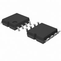
BU7262SF-E2 Rohm Semiconductor, BU7262SF-E2 Datasheet

BU7262SF-E2
Specifications of BU7262SF-E2
Available stocks
Related parts for BU7262SF-E2
BU7262SF-E2 Summary of contents
Page 1
... OUT 4 VSS SOP8 BU7262F BU7262SF BU7242F BU7242SF BU7261 G Single (BU7261SG:105 ℃ ) BU7262 F/FVM Dual (BU7262S F/FVM:105 ℃ ) BU7241 G Single (BU7261SG:105 ℃ ) BU7242 F/FVM Dual (BU7242S F/FVM:105 ℃ ) VDD 1 8 CH1 OUT2 IN2- CH2 IN2 MSOP8 BU7262FVM BU7262SFVM BU7242FVM BU7242SFVM 2007. Octber ...
Page 2
Absolute maximum rating(Ta=25[℃]) Parameter Symbol Supply Voltage VDD-VSS Differential Input Voltage(*1) Vid Input Common-mode voltage range Vicm Operating Temperature Topr Storage Temperature Tstg Maximum junction Temperature Tjmax Note: Absolute maximum rating item indicates the condition which must not be ...
Page 3
BU7261 family 800 600 BU7261G 400 200 100 AMBIENT TEMPERATURE [℃] Fig.1 Derating curve BU7261 family 1000 800 600 5.5V 3.0V 400 1.8V 200 0 -60 - ...
Page 4
BU7261 family 10.0 7.5 25℃ 5.0 -40℃ 2.5 0.0 105℃ 85℃ -2.5 -5.0 -7.5 -10 SUPPLY VOLTAGE [V] Fig.13 Input Offset Voltage – Supply Voltage (Vicm=VDD, VOUT=1.5[V]) BU7261 family 160 140 25℃ 40℃ ...
Page 5
... AMBIENT TEMPERATURE [℃] Fig.10 Output Source Current – Ambient Temperature (VOUT=VDD-0.4V) (*) The above date is ability value of sample not guaranteed. BU7262 F/FVM:-40[℃] to+85[℃] BU7262S F/FVM:-40[℃] to+105[℃] 1000 800 BU7262SF BU7262SFVM 600 400 200 0 150 0 50 100 AMBIENT TEMPERATURE [ ℃ ...
Page 6
BU7262 family 10.0 7.5 5.0 25℃ -40℃ 2.5 0.0 -2.5 105℃ 85℃ -5.0 -7.5 -10 SUPPLY VOLTAGE[V] Fig.13 Input Offset Voltage – Supply voltage (Vicm=VDD,VOUT=1.5[V]) BU7262 family 160 140 105℃ 85℃ 120 100 ...
Page 7
BU7241 family 800 600 BU7241G 400 200 100 AMBIENT TEMPERATURE [ ℃ ] Fig.1 Derating curve BU7241 family 250 200 5.5V 150 3.0V 100 1. -60 - SUPPLY ...
Page 8
BU7241 family 10.0 7.5 5.0 -40℃ 25℃ 2.5 0.0 105℃ 85℃ -2.5 -5.0 -7.5 -10 SUPPLY VOLTAGE [V] Fig.13 Input Offset Voltage – Supply Voltage (Vicm=VDD, VOUT=1.5[V]) BU7241 family 160 105℃ 140 85℃ ...
Page 9
BU7242 family 1000 800 BU7242F BU7242FVM 600 400 200 100 AMBIENT TEMPERATURE [ ℃ ] Fig.1 Derating curve BU7242 family 800 600 400 5.5V 3.0V 1.8V 200 0 -60 - ...
Page 10
BU7242 family 10.0 7.5 5.0 25℃ -40℃ 2.5 0.0 105℃ 85℃ -2.5 -5.0 -7.5 -10 SUPPLY VOLTAGE[V] Fig.13 Input Offset Voltage – Supply Voltage (Vicm=VDD, VOUT=1.5[V]) BU7242 family 160 140 105℃ 85℃ 120 ...
Page 11
Schematic diagram ● Test circuit1 NULL method VDD,VSS,EK,Vicm Unit : [V] VF Parameter VF1 Input offset voltage VF2 Large signal voltage gain VF3 VF4 Common-mode rejection ratio (Input common-mode voltage range) VF5 VF6 Power supply rejecyion ratio VF7 - ...
Page 12
Test circuit2 switch condition Unit: [V] SW No. Supply current maximum output voltage RL=10 [kΩ] output current Slew rate maximum frequency SW3 SW4 R2 100[kΩ] VDD=3[V] - SW1 + SW2 SW5 SW6 SW7 R1 1[kΩ] GND VIN- VIN+ Fig3. ...
Page 13
Description of electrical characteristics Described here are the terms of electric characteristics used in this technical note. Items and symbols used are also shown. Note that item name and symbol and their meaning may differ from those on another ...
Page 14
... Pd(max) θja2 < θja1 θja2 Tj(max) θja1 100 125 周囲温度 Ta[ ℃ ] BU7261/BU7241 Tj(max) (b) Derating curve BU7262F(*9) 620[mw] BU7242F(*9) BU7262FVM(*10) 480[mw] BU7242FVM(*10 100 150 AMBIENT TEMPERATURE [ ℃ ] BU7262SF(*9) 620[mw] BU7242SF(*9) BU7262SFVM(*10) 480[mw] BU7242SFVM(*10) 105 50 100 150 AMBIENT TEMPERATURE [ ℃ ] 150 ...
Page 15
Cautions on use 1) Absolute maximum ratings Absolute maximum ratings are the values which indicate the limits, within which the given voltage range can be safely charged to the terminal. However, it does not guarantee the circuit operation. 2) ...
Page 16
Dimensions SSOP5 ● Model number construction ・ Specify the product by the model number when placing an order. ・ Make sure of the combinations of items. ・ Start with the leftmost space without leaving any empty space between characters. ...
Page 17
Appendix No technical content pages of this document may be reproduced in any form or transmitted by any means without prior permission of ROHM CO.,LTD. The contents described herein are subject to change without notice. The specifications for the product ...


