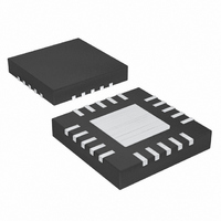
MAX6877ETG+ Maxim Integrated Products, MAX6877ETG+ Datasheet - Page 16

MAX6877ETG+
Manufacturer Part Number
MAX6877ETG+
Description
IC SEQUENCE/SUPERVISOR 24TQFN
Manufacturer
Maxim Integrated Products
Type
Sequencerr
Datasheet
1.MAX6878ETG.pdf
(24 pages)
Specifications of MAX6877ETG+
Number Of Voltages Monitored
3
Output
Open Drain or Open Collector
Reset
Active Low
Reset Timeout
Adjustable/Selectable
Voltage - Threshold
Adjustable/Selectable
Operating Temperature
-40°C ~ 85°C
Mounting Type
Surface Mount
Package / Case
24-TQFN Exposed Pad
Monitored Voltage
- 0.3 V to + 6 V
Manual Reset
Not Resettable
Watchdog
No Watchdog
Supply Voltage (max)
5.5 V
Supply Voltage (min)
2.7 V
Supply Current (typ)
1100 uA
Maximum Power Dissipation
1667 mW
Maximum Operating Temperature
+ 85 C
Mounting Style
SMD/SMT
Minimum Operating Temperature
- 40 C
Lead Free Status / RoHS Status
Lead free / RoHS Compliant
The MAX6877/MAX6878/MAX6879 multivoltage power
trackers/sequencers/supervisors monitor up to three
system voltages and provide proper power-up and
power-down control for systems requiring voltage
tracking or sequencing. These devices ensure con-
trolled voltage tracking with a specified range or
sequencing in the proper order as system power sup-
plies are enabled. The MAX6877/MAX6878/MAX6879
generate all required voltages and timing to control up
to three external n-channel pass FETs for the
OUT1/OUT2/OUT3 supply voltages (see the Selector
Guide for different features of each device.)
The MAX6877/MAX6878/MAX6879 feature adjustable
undervoltage thresholds for each input supply. When
all the voltages are above these adjusted thresholds,
the devices turn on the external n-channel MOSFETs to
either sequence or track the voltages to the system.
During the voltage-tracking mode, the voltage at the
GATE of each MOSFET is increased to slowly bring up
all supplies at a controlled slew rate. The voltage at the
source (output) of each MOSFET is internally compared
to a control ramp to maintain a low differential between
each monitored supply. Tracking is dynamically adjust-
ed to force all outputs to track within 125mV of the ref-
erence ramp. If for any reason any supplies fail to track
within ±250mV of the reference ramp, the FAULT out-
put is asserted, the power-up mode is terminated, and
all outputs are quickly powered off. In sequencing
mode, the outputs are turned on one after the other,
OUT1 first and OUT3 last. The MAX6877/MAX6878/
MAX6879 feature an autoretry or latch-off mode with
capacitor-adjusted timing.
These devices also provide a controlled power-down
(tracking mode) when the system shuts off in an orderly
manner. When an unexpected fault occurs, the outputs
are all pulled down simultaneously with an internal
100Ω pulldown to help discharge capacitive loads at
the MOSFET’s source.
The MAX6877/MAX6878/MAX6879 feature independent
internal charge pumps to fully enhance the external
FETs for low-voltage drops at highpass currents. The
MAX6877/MAX6878 also feature a power-good output
with a selectable timeout period that can be used for
system reset.
The MAX6877/MAX6878/MAX6879 monitor up to three
voltages. Devices may be configured to exclude any
IN_. To disable the tracking or sequencing operation of
any IN_, connect the IN_ to ground (or leave uncon-
nected) and connect SET_ to a voltage greater than
0.5V. The channel exclusion feature adds more flexibili-
Dual-/Triple-Voltage, Power-Supply
Trackers/Sequencers/Supervisors
16
______________________________________________________________________________________
Detailed Description
ty to the device in a variety of different applications. As
an example, the MAX6877 can track or sequence two
voltages using IN1 and IN2 while IN3 is left disabled.
These devices derive power from either the IN1, IN2, or
IN3 voltage inputs or V
V
ensure full device operation.
The highest input voltage on IN1/IN2/IN3 or V
plies power to the devices. Internal hysteresis ensures
that the supply input that initially powers these devices
continues to power the MAX6877/MAX6878/MAX6879
when multiple input voltages are within 100mV (typ) of
each other.
ABP powers the analog circuitry. Bypass ABP to GND
with a 1µF ceramic capacitor installed as close to the
device as possible. ABP takes the highest voltage of
IN_ or V
nal circuitry. ABP maintains the device supply voltage
during rapid power-down conditions.
To enable the power-up/power-down voltage-tracking
operation, drive TRK/SEQ low (connect TRK/SEQ to
GND). To enable power-up sequencing and power-
down tracking functions, drive TRK/SEQ high (connect
TRK/SEQ to ABP) or leave it unconnected. TRK/SEQ is
internally pulled to ABP through a 10µA current source
(see Figures 1 and 3).
To operate in tracking mode, connect TRK/SEQ to
GND. When V
above the internal SET_ threshold (0.5V), the tracking
process is initiated. The MAX6877/MAX6878/MAX6879
generate an internal reference ramp voltage that drives
the control loops for the tracked voltages. The tracking
functionality is monitored with a comparator control
block for each output (see the Functional Diagram).
The comparators monitor each OUT_ voltage with
respect to the common reference ramp voltage to
ensure the OUT_ voltages stay within 125mV of the ref-
erence ramp, monitor each tracked output voltage with
respect to its source input voltage, and monitor each
output voltage with respect to GND during power-
up/retry cycles. If for any reason any supplies fail to
track within ±250mV of the reference ramp, the FAULT
output is asserted, the power-up mode is terminated,
and all outputs are quickly powered off.
CC
or one of the IN_ inputs must be at least +2.7V to
CC
. Do not use ABP to provide power to exter-
Tracking and Sequencing Modes
EN/UV
MAX6877/MAX6878/MAX6879
> 1.25V and all SET_ inputs are
CC
(see the Functional Diagram).
Powering the
(
TRK /SEQ)
Tracking
CC
ABP
sup-


