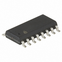
X40235S16I-A Intersil, X40235S16I-A Datasheet - Page 10

X40235S16I-A
Manufacturer Part Number
X40235S16I-A
Description
IC VOLTAGE MON TRPL EE 16-SOIC
Manufacturer
Intersil
Type
Multi-Voltage Supervisorr
Datasheet
1.X40231S16I-A.pdf
(36 pages)
Specifications of X40235S16I-A
Number Of Voltages Monitored
3
Output
Open Drain, Open Drain
Reset
Active High/Active Low
Reset Timeout
Adjustable/Selectable
Voltage - Threshold
1.75V, 2.2V, 2.95V
Operating Temperature
-40°C ~ 85°C
Mounting Type
Surface Mount
Package / Case
16-SOIC (0.300", 7.5mm Width)
Lead Free Status / RoHS Status
Contains lead / RoHS non-compliant
Depending upon the operation to be performed on
each of these individual parts, a 1, 2 or 3 Byte protocol
is used. All operations however must begin with the
Slave Address Byte being issued on the SDA pin. The
Slave address selects the part of the X4023x to be
addressed, and specifies if a Read or Write operation
is to be performed.
It should be noted that in order to perform a write oper-
ation to either a DCP or the EEPROM array, the Write
Enable Latch (WEL) bit must first be set (See “BL1,
BL0: Block Lock protection bits - (Nonvolatile)” on
page 18.)
Slave Address Byte
Following a START condition, the master must output
a Slave Address Byte (Refer to Figure 4). This byte
consists of three parts:
—The Device Type Identifier which consists of the most
—The next three bits (SA3 - SA1) are the Internal Device
—The Least Significant Bit of the Slave Address (SA0)
Nonvolatile Write Acknowledge Polling
After a nonvolatile write command sequence (for either
the EEPROM array, the Non Volatile Memory of a DCP
(NVM), or the CR Register) has been correctly issued
(including the final STOP condition), the X4023x ini-
tiates an internal high voltage write cycle. This cycle
typically requires 5 ms. During this time, no further
Read or Write commands can be issued to the device.
Write Acknowledge Polling is used to determine when
this high voltage write cycle has been completed.
significant four bits of the Slave Address (SA7 - SA4).
The Device Type Identifier must always be set to 1010
in order to select the X4023x.
Address bits. Setting these bits to 000 internally
selects the EEPROM array, while setting these bits to
111 selects the DCP structures in the X4023x. The CR
Register may be selected using the Internal Device
Address 010.
Byte is the R/W bit. This bit defines the operation to be
performed on the device being addressed (as defined
in the bits SA3 - SA1). When the R/W bit is “1”, then a
READ operation is selected. A “0” selects a WRITE
operation (Refer to Figure 4)
10
X40231, X40233, X40235, X40237, X40239
To perform acknowledge polling, the master issues a
START condition followed by a Slave Address Byte.
The Slave Address issued must contain a valid Inter-
nal Device Address. The LSB of the Slave Address
(R/W) can be set to either 1 or 0 in this case. If the
device is still busy with the high voltage cycle then no
ACKNOWLEDGE will be returned. If the device has
completed the write operation, an ACKNOWLEDGE
will be returned and the host can then proceed with a
read or write operation. (Refer to Figure 5)
DIGITALLY CONTROLLED POTENTIOMETERS
DCP Functionality
The X4023x includes one or two independent resistor
arrays. For the 64, 100 or 256 tap XDCPs, these
arrays respectively contain 63, 99 discrete resistive
segments that are connected in series. (the 256 tap
resistor achieves an equivalent end to end resistance.)
The physical ends of each array are equivalent to the
fixed terminals of a mechanical potentiometer. At one
end of the resistor array the terminal connects to the
R
is connected to V
Hx
pin (x = 0,1,2).The other end of the resistor array
Figure 4.
SA7
1 0 1 0
Internal Address
DEVICE TYPE
(SA3 - SA1)
IDENTIFIER
Bit SA0
SA6
000
010
111
0
1
SA5
SS
Slave Address Format
inside the package.
SA4
Internally Addressed
SA3
EEPROM Array
INTERNAL
ADDRESS
CR Register
DEVICE
SA2
Operation
Device
WRITE
DCP
READ
SA1
READ /
WRITE
R/W
SA0
April 11, 2005
FN8115.0


