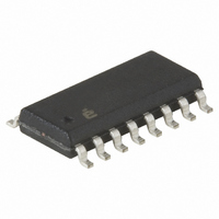
X40235S16I-AT1 Intersil, X40235S16I-AT1 Datasheet - Page 13

X40235S16I-AT1
Manufacturer Part Number
X40235S16I-AT1
Description
IC VOLTAGE MON TRPL EE 16-SOIC
Manufacturer
Intersil
Type
Multi-Voltage Supervisorr
Datasheet
1.X40231S16I-A.pdf
(36 pages)
Specifications of X40235S16I-AT1
Number Of Voltages Monitored
3
Output
Open Drain, Open Drain
Reset
Active High/Active Low
Reset Timeout
Adjustable/Selectable
Voltage - Threshold
1.75V, 2.2V, 2.95V
Operating Temperature
-40°C ~ 85°C
Mounting Type
Surface Mount
Package / Case
16-SOIC (0.300", 7.5mm Width)
Lead Free Status / RoHS Status
Contains lead / RoHS non-compliant
DCP Write Operation
A write to DCPx (x=0,1,2) can be performed using the
three byte command sequence shown in Figure 9.
In order to perform a write operation on a particular
DCP, the Write Enable Latch (WEL) bit of the CR Reg-
ister must first be set (See “BL1, BL0: Block Lock pro-
tection bits - (Nonvolatile)” on page 18.)
The Slave Address Byte 10101110 specifies that a
Write to a DCP is to be conducted. An ACKNOWL-
EDGE is returned by the X4023x after the Slave
Address, if it has been received correctly.
Next, an Instruction Byte is issued on SDA. Bits P1
and P0 of the Instruction Byte determine which WCR
is to be written, while the WT bit determines if the
Write is to be volatile or nonvolatile. If the Instruction
Byte format is valid, another ACKNOWLEDGE is then
returned by the X4023x.
Following the Instruction Byte, a Data Byte is issued to
the X4023x over SDA. The Data Byte contents is
latched into the WCR of the DCP on the first rising
edge of the clock signal, after the LSB of the Data Byte
(D0) has been issued on SDA (See Figure 34).
The Data Byte determines the “wiper position” (which
FET switch of the DCP resistive array is switched ON)
of the DCP. The maximum value for the Data Byte
depends upon which DCP is being addressed (see fol-
lowing table).
P1- P0
0
0
1
1
S
T
A
R
T
0
1
0
1
1
0
DCPx
x = 0
x = 1
x = 2
SLAVE ADDRESS BYTE
1
0
1
# Taps
256
100
13
64
1
Reserved
1
X40231, X40233, X40235, X40237, X40239
Figure 9.
0
Refer to Appendix 1
Max. Data Byte
A
C
K
WT
3Fh
FFh
DCP Write Command Sequence
0
INSTRUCTION BYTE
0
0
0
0
Using a Data Byte larger than the values specified
above results in the “wiper terminal” being set to the
highest tap position. The “wiper position” does NOT
roll-over to the lowest tap position.
For DCP0 (64 Tap) and DCP2 (256 Tap), the Data
Byte maps one to one to the “wiper position” of the
DCP “wiper terminal”. Therefore, the Data Byte
00001111 (15
minal” to tap position 15. Similarly, the Data Byte
00011100 (28
minal” to tap position 28. The mapping of the Data
Byte to “wiper position” data for DCP1 (100 Tap), is
shown in “APPENDIX 1” . An example of a simple C
language function which “translates” between the tap
position (decimal) and the Data Byte (binary) for
DCP1, is given in “APPENDIX 2” .
It should be noted that all writes to any DCP of the
X4023x are random in nature. Therefore, the Data
Byte of consecutive write operations to any DCP can
differ by an arbitrary number of bits. Also, setting the
bits P1 = 1, P0 = 1 is a reserved sequence, and will
result in no ACKNOWLEDGE after sending an Instruc-
tion Byte on SDA.
The factory default setting of all “wiper position” set-
tings is with 00h stored in the NVM of the DCPs. This
corresponds to having the “wiper terminal” R
(x = 0,1,2) at the “lowest” tap position, Therefore, the
resistance between R
(essentially only the Wiper Resistance, R
P1 P0
A
C
K
D7 D6 D5 D4 D3 D2 D1 D0
10
10
) corresponds to setting the “wiper ter-
) corresponds to setting the “wiper ter-
DATA BYTE
WX
and R
LX
is a minimum
W
).
A
C
K
April 11, 2005
S
T
O
P
FN8115.0
WX


