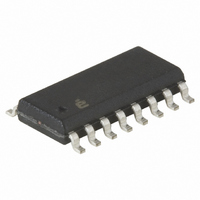
X40237S16I-BT1 Intersil, X40237S16I-BT1 Datasheet - Page 11

X40237S16I-BT1
Manufacturer Part Number
X40237S16I-BT1
Description
IC VOLTAGE MON TRPL EE 16-SOIC
Manufacturer
Intersil
Type
Multi-Voltage Supervisorr
Datasheet
1.X40231S16I-A.pdf
(36 pages)
Specifications of X40237S16I-BT1
Number Of Voltages Monitored
3
Output
Open Drain, Open Drain
Reset
Active High/Active Low
Reset Timeout
Adjustable/Selectable
Voltage - Threshold
1.75V, 2.95V, 4.45V
Operating Temperature
-40°C ~ 85°C
Mounting Type
Surface Mount
Package / Case
16-SOIC (0.300", 7.5mm Width)
Lead Free Status / RoHS Status
Contains lead / RoHS non-compliant
REGISTER
COUNTER
VOLATILE
MEMORY
Figure 5.
WIPER
(NVM)
(WCR)
NON
Figure 6.
command sequence?
Issue Slave Address
Byte (Read or Write)
Byte load completed
High Voltage Cycle
complete. Continue
command sequence
Enter ACK Polling
by issuing STOP.
Continue normal
Issue START
Read or Write
PROCEED
returned?
DECODER
Acknowledge Polling Sequence
ACK
DCP Internal Structure
N
YES
YES
2
1
0
11
SWITCHES
“WIPER”
FET
X40231, X40233, X40235, X40237, X40239
NO
NO
Issue STOP
RESISTOR
ARRAY
Issue STOP
R
R
Hx
Wx
At both ends of each array and between each resistor
segment there is a CMOS switch connected between
the resistor array and the wiper (R w
each individual array, only one switch may be turned
on at any one time. These switches are controlled by
the Wiper Counter Register (WCR) (See Figure 6).
The WCR is a volatile register.
On power-up of the X4023x, wiper position data is au-
tomatically loaded into the WCR from its associated
Non Volatile Memory (NVM) Register. The Table below
shows the Initial Values of the DCP WCR’s before the
contents of the NVM is loaded into the WCR.
The data in the WCR is then decoded to select and
enable one of the respective FET switches. A “make
before break” sequence is used internally for the FET
switches when the wiper is moved from one tap posi-
tion to another.
Hot Pluggability
Figure 7 shows a typical waveform that the X4023x
might experience in a Hot Pluggable situation. On
power-up, V
some amount of ringing, before it settles to the
required value.
The device is designed such that the wiper terminal
(R
stored in the DCP NVM), when the voltage applied to
V
Power-on Reset time, set in the CR Register - See
“CONTROL AND STATUS REGISTER” on page 18.).
Therefore, if
to settle above V
wiper terminal position is recalled by (a maximum)
time:
determined by system hot plug conditions.
DCP Operations
In total there are three operations that can be per-
formed on any internal DCP structure:
—DCP Nonvolatile Write
—DCP Volatile Write
—DCP Read
CC
Wx
R
R
R
1
2
0
exceeds V
) is recalled to the correct position (as per the last
(100 TAP)
(256 TAP)
t
(64 TAP)
DCP
trans
+
CC
t
trans
t
PURST
TRIP1
applied to the X4023x may exhibit
TRIP1
is defined as the time taken for V
. It should be noted that
for a time exceeding t
Initial Values Before Recall
(Figure 7): then the desired
V
V
V
H
H
L
(TAP = 255)
(TAP = 63)
(TAP = 0)
x
) output. Within
PURST
April 11, 2005
t
trans
FN8115.0
(the
CC
is


