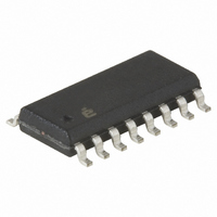
X40237S16I-BT1 Intersil, X40237S16I-BT1 Datasheet - Page 12

X40237S16I-BT1
Manufacturer Part Number
X40237S16I-BT1
Description
IC VOLTAGE MON TRPL EE 16-SOIC
Manufacturer
Intersil
Type
Multi-Voltage Supervisorr
Datasheet
1.X40231S16I-A.pdf
(36 pages)
Specifications of X40237S16I-BT1
Number Of Voltages Monitored
3
Output
Open Drain, Open Drain
Reset
Active High/Active Low
Reset Timeout
Adjustable/Selectable
Voltage - Threshold
1.75V, 2.95V, 4.45V
Operating Temperature
-40°C ~ 85°C
Mounting Type
Surface Mount
Package / Case
16-SOIC (0.300", 7.5mm Width)
Lead Free Status / RoHS Status
Contains lead / RoHS non-compliant
A nonvolatile write to a DCP will change the “wiper posi-
tion” by simultaneously writing new data to the associ-
ated WCR and NVM. Therefore, the new “wiper position”
setting is recalled into the WCR after V
is powered down and then powered back up.
A volatile write operation to a DCP however, changes
the “wiper position” by writing new data to the associ-
ated WCR only. The contents of the associated NVM
register remains unchanged. Therefore, when V
the device is powered down then back up, the “wiper
position” reverts to that last position written to the DCP
using a nonvolatile write operation.
Both volatile and nonvolatile write operations are exe-
cuted using a three byte command sequence: (DCP)
Slave Address Byte, Instruction Byte, followed by a
Data Byte (See Figure 9)
A DCP Read operation allows the user to “read out”
the current “wiper position” of the DCP, as stored in
the associated WCR. This operation is executed using
the Random Address Read command sequence, con-
sisting of the (DCP) Slave Address Byte followed by
an Instruction Byte and the Slave Address Byte again
(Refer to Figure 10).
Instruction Byte
While the Slave Address Byte is used to select the
DCP devices, an Instruction Byte is used to determine
which DCP is being addressed.
The Instruction Byte (Figure 8) is valid only when the
Device Type Identifier and the Internal Device Address
bits of the Slave Address are set to 1010111. In this
case, the two Least Significant Bit’s (I1 - I0) of the
Instruction Byte are used to select the particular DCP
(0 - 2). In the case of a Write to any of the DCPs (i.e.
V
CC
0
t
TRANS
12
X40231, X40233, X40235, X40237, X40239
CC
of the X4023x
Figure 7.
CC
t
PURST
to
DCP Power-up
the LSB of the Slave Address is 0), the Most Signifi-
cant Bit of the Instruction Byte (I7), determines the
Write Type (WT) performed.
If WT is “1”, then a Nonvolatile Write to the DCP occurs.
In this case, the “wiper position” of the DCP is changed
by simultaneously writing new data to the associated
WCR and NVM. Therefore, the new “wiper position”
setting is recalled into the WCR after V
has been powered down then powered back up.
If WT is “0” then a DCP Volatile Write is performed.
This operation changes the DCP “wiper position” by
writing new data to the associated WCR only. The
contents of the associated NVM register remains
unchanged. Therefore, when V
powered down then back up, the “wiper position”
reverts to that last written to the DCP using a nonvol-
atile write operation.
†
WT
This bit has no effect when a Read operation is being performed.
0
1
WRITE TYPE
†
Figure 8.
Select a Volatile Write operation to be performed
I7
WT
formed on the DCP pointed to by bits P1 and P0
Maximum Wiper Recall time
Select a Nonvolatile Write operation to be per-
on the DCP pointed to by bits P1 and P0
I6
0
I5
0
Instruction Byte Format
V
V
CC (Max.)
TRIP1
I4
0
Description
t
I3
0
I2
CC
0
DCP SELECT
to the device is
CC
I1
P1
of the X4023x
I0
P0
April 11, 2005
FN8115.0


