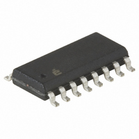
X40237S16I-BT1 Intersil, X40237S16I-BT1 Datasheet - Page 8

X40237S16I-BT1
Manufacturer Part Number
X40237S16I-BT1
Description
IC VOLTAGE MON TRPL EE 16-SOIC
Manufacturer
Intersil
Type
Multi-Voltage Supervisorr
Datasheet
1.X40231S16I-A.pdf
(36 pages)
Specifications of X40237S16I-BT1
Number Of Voltages Monitored
3
Output
Open Drain, Open Drain
Reset
Active High/Active Low
Reset Timeout
Adjustable/Selectable
Voltage - Threshold
1.75V, 2.95V, 4.45V
Operating Temperature
-40°C ~ 85°C
Mounting Type
Surface Mount
Package / Case
16-SOIC (0.300", 7.5mm Width)
Lead Free Status / RoHS Status
Contains lead / RoHS non-compliant
DETAILED DEVICE DESCRIPTION
The X4023x combines One or Two Intersil Digitally
Controlled
power-on reset control, V
two supplementary voltage monitors with independent
outputs, and integrated EEPROM with Block Lock™
protection, in one package. The integrated functional-
ity of the X4023x lowers system cost, increases reli-
ability, and reduces board space requirements.
DCPs allow for the “set-and-forget” adjustment during
production test or in-system updating via the industry
standard 2-wire interface.
Applying voltage to V
circuit which sets the RESET output HIGH, until the
supply voltage stabilizes for a period of time (50-300
msec selectable via software). The RESET output then
goes LOW. The Low Voltage Reset circuit sets the
RESET output HIGH when V
mum V
returns to proper operating level and stabilizes for a
period of time (t
allows the user to externally activate the RESET output.
Two supplementary Voltage Monitor circuits, V2MON
and V3MON, continuously compare their inputs to
individual trip voltages (independent on-chip voltage
references factory set and user programmable). When
an input voltage exceeds it’s associated trip level, the
corresponding output (V3FAIL, V2FAIL) goes HIGH.
When the input voltage becomes lower than it’s asso-
ciated trip level, the corresponding output is driven
LOW. A corresponding binary representation of the
two monitor circuit outputs (V2FAIL and V3FAIL) are
also stored in latched, volatile (CR) register bits. The
status of these two monitor outputs can be read out via
the 2-wire serial port. The bits will remain SET, even
after the alarm condition is removed, allowing
advanced recovery algorithms to be implemented.
CC
trip point. RESET remains HIGH until V
Potentiometer
SDA
SCL
PURST)
CC
. A Manual Reset (MR) input
activates the Power-on Reset
CC
8
low voltage reset control,
(XDCP)
Figure 1.
CC
X40231, X40233, X40235, X40237, X40239
falls below the mini-
Data Stable
devices,
Valid Data Changes on the SDA Bus
V
CC
CC
Data Change
Intersil’s unique circuits allow for all internal trip voltages
to be individually programmed with high accuracy,
either by Intersil at final test or by the user during their
production process. Some distributors offer V
reprogramming as a value added service. This gives
the designer great flexibility in changing system param-
eters, either at the time of manufacture, or in the field.
The memory portion of the device is a CMOS serial
EEPROM array with Intersil’s Block Lock
This memory may be used to store module manufactur-
ing data, serial numbers, or various other system
parameters. The EEPROM array is internally organized
as x 8, and utilizes Intersil’s proprietary Direct Write
cells providing a minimum endurance of 1,000,000
cycles and a minimum data retention of 100 years.
The device features a 2-Wire interface.
PRINCIPLES OF OPERATION
SERIAL INTERFACE
Serial Interface Conventions
The device supports a bidirectional bus oriented proto-
col. The protocol defines any device that sends data
onto the bus as a transmitter, and the receiving device
as the receiver. The device controlling the transfer is
called the master and the device being controlled is
called the slave. The master always initiates data
transfers, and provides the clock for both transmit and
receive operations. The X4023x operates as a slave in
all applications.
Serial Clock and Data
Data states on the SDA line can change only while
SCL is LOW (see Figure 1). SDA state changes while
SCL is HIGH are reserved for indicating START and
STOP conditions. See Figure 1. On power-up of the
X4023x, the SDA pin is in the input mode.
Data Stable
TM
protection.
April 11, 2005
FN8115.0
TRIP
TM


