BD3951F-E2 Rohm Semiconductor, BD3951F-E2 Datasheet
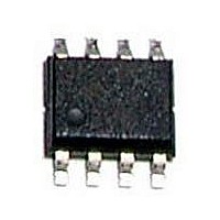
IC REG LDO W/VOLT DETECT 8SOP

BD3951F-E2

Manufacturer Part Number
BD3951F-E2
Description
IC REG LDO W/VOLT DETECT 8SOP
Manufacturer
Rohm Semiconductor
Datasheets

Specifications of BD3951F-E2

Regulator Topology
Positive Fixed
Voltage - Output
5V
Voltage - Input
6 ~ 20 V
Voltage - Dropout (typical)
0.31V @ 100mA
Number Of Regulators
1
Current - Output
150mA (Min)
Operating Temperature
-40°C ~ 125°C
Mounting Type
Surface Mount
Package / Case
8-SOP
Primary Input Voltage
13.5V
Output Voltage
5.1V
Dropout Voltage Vdo
310mV
No. Of Pins
8
Output Current
150mA
Voltage Regulator Case Style
SOP
Operating Temperature Range
-40°C To +125°C
Svhc
No
Mounting Style
SMD/SMT
Output Voltage Fixed
5.1V
Rohs Compliant
Yes
Lead Free Status / RoHS Status
Lead free / RoHS Compliant
Current - Limit (min)
-
Lead Free Status / Rohs Status
Lead free / RoHS Compliant

Available stocks

Company
Part Number
Manufacturer
Quantity
Price
Part Number:
BD3951F-E2
Manufacturer:
ROHM/罗姆
Quantity:
20 000
Power Management LSI Series for Automotive Body Control
Regulator with Voltage
Detector IC
BD3951F
●Description
●Features
●Applications
●Absolute Maximum Ratings (Ta=25℃)
BD3951F is a 5V LDO system regulator particularly developed for automotive applications. The output current of the
regulator can be drawn up to 150mA, and it has built-in power-on reset and input voltage sense. This device can withstand
50V surge input voltage as well as wide ambient temperature operations from -40℃ to +125℃. The adjustable reset
delay time and detection input voltage allow to meet with wide range of design requirements.
*1 tr (rising time) is over 1msec, applied voltage is less than 400msec
*2 Pd is derated at 5.5mW/℃ for temperature above Ta=25℃, mounted on 70mm×70mm×1.6mm PCB.
*3 Input current from Vcc to SIN PIN has to be equal and less than 5mA when Vcc voltage is less than SIN PIN voltage.
Vcc Input Voltage
Out Terminal Voltage
RES Terminal Voltage
SOUT Terminal Voltage
RES Output Current
SOUT Output Current
SIN Input Voltage
Power Dissipation
Operating Temperature Range
Storage Temperature Range
Vcc Peak Input Voltage
·Automotive application (Rain Sensor and Cluster Panel etc.) and all other electronics application.
1) Micro processor power supply 5.0V, Adjustable Reset, Adjustable Comparator.
2) 5V is Pch DMOS type low drop out voltage regulator. Iomax=150mA.
3) Low ESR capacitor (Ceramic Capacitor) is available for the Output Capacitor.
4) Over Current Protection built in to prevent the destruction of IC.
5) Thermal Shut Down is built in to prevent the heat runaway.
6) VCC absolute Maximum Ratings 36V.
7) Vcc peak input voltage 50V (*1)
8) Small surface mount package SOP8.
Parameter
TECHNICAL NOTE
Vccpeak
Symbol
Vsout
Isout
Vout
Vres
Vsin
Topr
Tstg
Vcc
Ires
Pd
-0.3~+36 *3
-40~+125
-55~+150
-0.3~+36
-0.3~+7
-0.3~+7
-0.3~+7
687 *2
Limit
0.2
2.5
50
Unit
mA
mA
mV
V
V
V
V
V
V
Dec. 2006

Related parts for BD3951F-E2

BD3951F-E2 Summary of contents

Page 1

... BD3951F ●Description BD3951F LDO system regulator particularly developed for automotive applications. The output current of the regulator can be drawn up to 150mA, and it has built-in power-on reset and input voltage sense. This device can withstand 50V surge input voltage as well as wide ambient temperature operations from -40℃ to +125℃. The adjustable reset delay time and detection input voltage allow to meet with wide range of design requirements. ● ...

Page 2

Conditions (Ta=-40℃~+125℃) Parameter Recommended Supply Voltage *4 Operatinal Supply Voltage *5 Reset Adjustable Range Reset Delay Time Controllable Range Vcc Detection Adjustable Range *4 The range within test condition of the electrical characteristics. *5 The range exceeding the test ...

Page 3

Data(Unless otherwise specified Ta=-40℃~+125℃,Vcc=13.5V) -40℃ 25℃ 125℃ SUPPLY VOLTAGE: Vcc [V] Fig.1 Circuit Current 1 * Vcc=4.75V 0.8 0.6 125℃ 0.4 25℃ -40℃ 0 ...

Page 4

Diagram, Application Circuit, Pin Description Vcc 1 PreReg 0.33μF Vref R2:36kΩ R1:10kΩ VCC RADJ 3 VCC 2 SIN GND 5 Fig.13 ・ ESR range of the output capacitor (ceramic capacitor) to 100Ω. ・ VCC must be ...

Page 5

Circuit SIN(2pin) Vcc 200k SIN(2pin) RES(6pin) OUT(8pin) 20k RES(6pin) ● How to set RESET delay time using CT terminal capacitor There are three factors to define the RESET delay time TdLH. External capacitor value Cct of the CT ...

Page 6

... Therefore physical safety guard, like fuse, is recommended to prevent unexpected extreme condition which might beyond absolute maximum ratings. 2. BD3951F can operate within the operating supply voltage range and operating temperature range. The Limits over the input voltage is not warranted, however electric characteristics curve in operating condition should be within the expected linearity. ...

Page 7

... BD3951F might be damaged from the exceed inflow current from the terminals to VCC (for instance, VCC is short to GND while the output capacitor is charging.). In those cases, VCC series diode (to prevent inflow current) or bypass diode (connected from terminals to VCC) should be used externally in an application ...

Page 8

Selecting a Model Name When Ordering Part number ROHM model name SOP8 <Dimension> 5.0±0 0.15±0.1 0.1 1.27 0.4±0.1 The contents described herein are correct as of December, 2006 The contents described herein ...

Page 9

Appendix No technical content pages of this document may be reproduced in any form or transmitted by any means without prior permission of ROHM CO.,LTD. The contents described herein are subject to change without notice. The specifications for the product ...

Related keywords