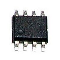
BD3951F-E2 Rohm Semiconductor, BD3951F-E2 Datasheet - Page 6

BD3951F-E2
Manufacturer Part Number
BD3951F-E2
Description
IC REG LDO W/VOLT DETECT 8SOP
Manufacturer
Rohm Semiconductor
Specifications of BD3951F-E2
Regulator Topology
Positive Fixed
Voltage - Output
5V
Voltage - Input
6 ~ 20 V
Voltage - Dropout (typical)
0.31V @ 100mA
Number Of Regulators
1
Current - Output
150mA (Min)
Operating Temperature
-40°C ~ 125°C
Mounting Type
Surface Mount
Package / Case
8-SOP
Primary Input Voltage
13.5V
Output Voltage
5.1V
Dropout Voltage Vdo
310mV
No. Of Pins
8
Output Current
150mA
Voltage Regulator Case Style
SOP
Operating Temperature Range
-40°C To +125°C
Svhc
No
Mounting Style
SMD/SMT
Output Voltage Fixed
5.1V
Rohs Compliant
Yes
Lead Free Status / RoHS Status
Lead free / RoHS Compliant
Current - Limit (min)
-
Lead Free Status / Rohs Status
Lead free / RoHS Compliant
Available stocks
Company
Part Number
Manufacturer
Quantity
Price
Part Number:
BD3951F-E2
Manufacturer:
ROHM/罗姆
Quantity:
20 000
●Thermal Design
effect from operating ambient temperature.
degrade or be demolished permanently.
reliability.
To prevent thermal destroy, IC must be operated under the condition that junction temperature is less than Tjmax. SOP8
package power dissipation temperature de-rating curve is shown in Fig. 17. Operating condition must be less than power
dissipation curve. Calculation formula is as below.
Derive IOUT as operation is less than power dissipation curve,
IOUT max is defined by Vcc and VOUT.
·Example
Power consumption (Pc) has to be less than power dissipation curve along with the temperature.
The equation under short circuit condition (VOUT-GND short) is as below.
●Notes for use
1.
2.
3.
4.
5.
Please consider about power dissipation de-rating curve for high temperature operations. IC characteristics receive great
Ta=85℃, Vcc=13.5V and VOUT=5V
Pc=(Vcc-VOUT)×IOUT+Vcc×Icc
Power Dissipation Pd ≤ Pc
IOUT ≤
IOUT ≤
IOUT≤41.8mA (Icc=135µA)
Pc=Vcc×(Icc+Ishort) Ishort=Short Current
This product are produced with strict quality control, but might be destroyed in using beyond absolute maximum ratings.
The destroyed IC failure mode cannot be defined (like Short mode, or Open mode).
Therefore physical safety guard, like fuse, is recommended to prevent unexpected extreme condition which might beyond
absolute maximum ratings.
BD3951F can operate within the operating supply voltage range and operating temperature range.
The Limits over the input voltage is not warranted, however electric characteristics curve in operating condition should be
within the expected linearity.
GND terminal voltage must be always forced with the lowest voltage among the terminals.
Power GND pattern and Small signal GND pattern should be separated each other and is recommended to supply one
point GND on the board to eliminate the surge current influences. External components GND pattern should not be long
to avoid electrical interferences.
For thermal design, refer to the thermal de-rating characteristics and be sure to use this IC within the power dissipation
range at any conditions.
0.357-13.5×Icc
Pd-Vcc×Icc
Vcc-VOUT
13.5-5
1000
800
600
400
200
(Icc is shown in Fig. 1)
687
0
0
25
Heat design should take consideration from both instant demolish and long life
Glass Epoxy Board
Mount Condition Θj-a=181.8 (℃/W)
θja=181.8℃/W→-5.5mW/℃
25℃=687mW→85℃=357mW
If junction temperature exceeds rating temperature (Tjmax), device might
50
Ta
Fig.17
75
(70mm×70mm×1.6mm)
[
℃
6/8
100
]
125
VOUT : Output Voltage
150
IOUT : Output Current
Vcc : Input Voltage
Icc : Circuit Current


