LD1084D2T12R STMicroelectronics, LD1084D2T12R Datasheet
LD1084D2T12R
Specifications of LD1084D2T12R


Related parts for LD1084D2T12R


LD1084D2T12R Summary of contents
Page 1
A low drop positive voltage regulator adjustable Features ■ Typical dropout 1 ■ Three terminal adjustable output voltage ■ Guaranteed output current ■ Output tolerance ± °C ...
Page 2
Contents 1 Diagram . . . . . . . . . . . . . . . . . . . . . . . . . . . . . . . . . . . . . ...
Page 3
Diagram Figure 1. Schematic diagram Doc ID 9035 Rev 9 3/16 ...
Page 4
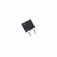
Pin configuration Figure 2. Pin connections (top view) 4/16 Doc ID 9035 Rev 9 ...
Page 5
Maximum ratings Table 2. Absolute maximum ratings Symbol V DC input voltage I I Output current O P Power dissipation D T Storage temperature range STG T Operating junction temperature range OP Note: Absolute maximum ratings are those values ...
Page 6
Schematic application Figure 3. Application circuit 6/ Doc ID 9035 Rev 9 R ⎛ ⎞ 2 ⋅ ------ - ⎝ ⎠ REF R 1 ...
Page 7
Electrical characteristics Table 4. Electrical characteristics of LD1084XX Symbol Parameter (1) V Output voltage O ΔV Line regulation O ΔV Load regulation O V Dropout voltage d I Minimum load ...
Page 8
Typical application Unless otherwise specified T Figure 4. Short circuit current vs. dropout voltage Figure 6. Quiescent current vs. temperature Figure 8. Load regulation vs. temperature 8/ ° µF (tant.), ...
Page 9
Figure 10. Quiescent current vs. input voltage Figure 11. Dropout voltage vs. output current Figure 12. Supply voltage rejection vs. output current Figure 14. Supply voltage rejection vs. temperature Figure 13. Dropout voltage vs. temperature Figure 15. Supply voltage rejection ...
Page 10
Figure 16. Adjust pin current vs. output current Figure 18. Load regulation vs. temperature Figure 20. Line regulation vs. temperature 10/16 Figure 17. Reference voltage vs. temperature Figure 19. Adjust pin current vs. temperature Figure 21. Minimum load current vs. ...
Page 11
Figure 22. Supply voltage rejection vs. temperature Figure 24. Stability Figure 26. Stability Figure 23. Supply voltage rejection vs. frequency Figure 25. Supply voltage rejection vs. output current Figure 27. Line transient V =14 to 15V, I =200mA ...
Page 12
Figure 28. Line transient V =12 to 13V, I =200mA 1µF(tant =5µs ADJ s f Figure 30. Load transient 1µF(tant), C ...
Page 13
Package mechanical data In order to meet environmental requirements, ST offers these devices in different grades of ® ECOPACK packages, depending on their level of environmental compliance. ECOPACK specifications, grade definitions and product status are available at: www.st.com. ® ...
Page 14
Dim. Min. A 4.40 C 1. 0.49 F 0.61 F1 1.14 F2 1.14 G 4.95 G1 2 13.0 L5 2.65 L6 15.25 L7 6.2 L9 3.5 DIA. 3.75 14/16 TO-220 mechanical data ...
Page 15
Revision history Table 5. Document revision history Date Revision 07-Oct-2004 3 08-Feb-2005 4 16-Jun-2005 5 04-Apr-2007 6 07-Jun-2007 7 08-Apr-2008 8 29-Jul-2009 9 Changes Mistake order codes - Table 1. Mistake U.M. Load Regulation - V ==> mV. Order ...
Page 16
... Information in this document is provided solely in connection with ST products. STMicroelectronics NV and its subsidiaries (“ST”) reserve the right to make changes, corrections, modifications or improvements, to this document, and the products and services described herein at any time, without notice. All ST products are sold pursuant to ST’s terms and conditions of sale. ...