USBULC6-2F3 STMicroelectronics, USBULC6-2F3 Datasheet
USBULC6-2F3
Specifications of USBULC6-2F3
USBULC6-2F3
Available stocks


Related parts for USBULC6-2F3


USBULC6-2F3 Summary of contents
Page 1
... High speed USB port in wireless handsets (up to 480 Mb/s according to USB 2.0 high speed specification) Description The USBULC6-2F3 is a monolithic, application specific discrete device dedicated to ESD protection of high speed interfaces. Its ultra low line capacitance secures a high level of signal integrity without compromizing the protection of downstream sensitive chips against the most stringently characterized ESD strikes ...
Page 2
... Voltage temperature coefficient V Forward voltage drop F Symbol Exponential wave form 8/20 µ line LINE 2/9 amb Parameter = 25 °C) amb Parameter RM Test conditions = mV MHz OSC USBULC6-2F3 = 25 °C) Value 125 - -55 to +150 Slope = 1/ Min. Typ. Max 100 1.6 5 1.2 Unit kV W °C °C ° ...
Page 3
... Figure 4. Eye diagram, board with USBULC6-2F3 (according to USB 2.0 high speed specification) USBULC6-2F3 480 Mb/s Horiz: 350 ps/div Ver: 200 mV/div Figure 6. ESD response to IEC 61000-4-2 (-15 kV air discharge) Figure 8. Analog crosstalk measurement dB 0 ...
Page 4
... F (Hz) -10.00 100.0k 1.0M 10.0M 100.0M Rise time = 1.647 205 mV pkpk Figure 12. Peak pulse power versus 1000 100 10 100 125 150 1 USBULC6-2F3 1.0G INPUT: 1 V/div 0 mV offset 2 ns/div 5 Gs/s OUTPUT: 100 m V/div -300 mV offset 2 ns/div 5 Gs/s exponential pulse duration (µ initial = 25° ...
Page 5
... USBULC6-2F3 Figure 13. Clamping voltage versus peak pulse current (typical values, exponential waveform) 100.0 10.0 1.0 V ( Application information Figure 15. Application diagram USB CONNECTOR Vbus GND Figure 14. Relative variation of leakage 1.E+02 1.E+01 8/20 µs T initial =25° 1.E+ Vbus GND Application information ...
Page 6
... ECOPACK trademark. ECOPACK specifications are available at www.st.com. Figure 17. Package dimensions 260 µm 6/9 MIN ead-free, pitch = 400 µm, bump = 255 µm 400 µm ± 40 255 µm ± 40 0.92 mm ± 30 µm USBULC6-2F3 USB ULC ® 605 µm ± 55 ...
Page 7
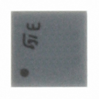
... More information is available in the application notes: AN2348: “400 µm Flip Chip: Package description and recommendations for use” AN1751: "EMI Filters: Recommendations and measurements" 5 Ordering information Table 3. Ordering information Order code USBULC6-2F3 Figure 19. Marking Dot identifying Pin A1 location 0.71 User direction of unreeling Marking Package EH ...
Page 8
... Revision history 6 Revision history Table 4. Document revision history Date 15-Dec-2006 29-Apr-2008 8/9 Revision 1 Initial release. Updated ECOPACK statement. Updated 2 Figure 20. Reformatted to current standards. USBULC6-2F3 Changes Figure 17, Figure 18 and ...
Page 9
... USBULC6-2F3 Information in this document is provided solely in connection with ST products. STMicroelectronics NV and its subsidiaries (“ST”) reserve the right to make changes, corrections, modifications or improvements, to this document, and the products and services described herein at any time, without notice. All ST products are sold pursuant to ST’s terms and conditions of sale. ...