IP4085CX4/LF,135 NXP Semiconductors, IP4085CX4/LF,135 Datasheet
IP4085CX4/LF,135
Specifications of IP4085CX4/LF,135


Related parts for IP4085CX4/LF,135


IP4085CX4/LF,135 Summary of contents
Page 1
IP4085CX4; IP4385CX4; IP4386CX4; IP4387CX4 Integrated high-performance ESD-protection diodes to IEC61000-4-2, level 4 Rev. 01 — 26 March 2009 1. Product profile 1.1 General description IP4085CX4, IP4385CX4, IP4386CX4 and IP4387CX4 are designed to protect appliances from destruction by either: • ElectroStatic ...
Page 2
... NXP Semiconductors 2. Pinning information Fig 1. Table 1. Pin A1 and A2 B1 and B2 3. Ordering information Table 2. Ordering information Type number Package Name Description IP4085CX4/LF WLCSP4 wafer level chip-size package: 4 bumps; 0.91 IP4385CX4/LF WLCSP4 wafer level chip-size package: 4 bumps; 0.76 IP4386CX4/LF WLCSP4 wafer level chip-size package: 4 bumps; 0.76 ...
Page 3
... NXP Semiconductors 5. Limiting values Table 3. Limiting values In accordance with the Absolute Maximum Rating System (IEC 60134). Symbol Parameter V supply voltage CC V electrostatic discharge voltage ESD I peak pulse current PP I non-repetitive peak forward FSM current P total power dissipation tot IP4085_4385_4386_4387_CX4_1 Product data sheet ...
Page 4
... NXP Semiconductors Table 3. Limiting values …continued In accordance with the Absolute Maximum Rating System (IEC 60134). Symbol Parameter T storage temperature stg T peak reflow temperature reflow(peak) T ambient temperature amb [1] Device tested with over 1000 pulses contact discharges, according to the IEC 61000-4-2 model. [2] Severe self-heating demands a heat-dissipation optimized PCB to prevent the device from de-soldering. For ambient temperatures above 50 C, the guaranteed life time is 48 hours at 0 ...
Page 5
... NXP Semiconductors Table 5. Electrical characteristics unless otherwise specified. amb Symbol Parameter C diode capacitance d IP4085CX4 IP4385CX4 IP4386CX4 IP4387CX4 V diode forward voltage Fd IP4085CX4 IP4385CX4 IP4386CX4 IP4387CX4 8. Application information 8.1 Forward current DC clamping voltage The forward current DC clamping voltage is of interest when protecting circuits from voltage sources with the wrong polarity ...
Page 6
... NXP Semiconductors 1 (V) 1.0 0.9 0.8 0.7 0 0.2 0.4 ( +25 C. amb ( +85 C. amb ( amb Fig 4. DC clamping voltage as a function of forward current; IP4085CX4 1 (V) 1.0 0.9 0.8 0.7 0 0.2 0.4 ( +25 C. amb ( +85 C. amb ( amb Fig 6. DC clamping voltage as a function of forward current ...
Page 7
... NXP Semiconductors 8.2 Peak clamping voltage The peak clamping voltage for forward and reverse current pulses of 8/20 s (IEC 61000-4-5) is significant when protecting circuits from power surges due to voltage discharges. The current pulse shape over time is shown in measurement setup for forward current and reverse current pulses respectively are shown ...
Page 8
... NXP Semiconductors 17 V CL(M) ( +25 C. amb ( +85 C. amb ( amb Fig 10. Peak clamping voltage as a function of forward current; IP4085CX4 20 V CL( +25 C. amb ( +85 C. amb ( amb Fig 12. Peak clamping voltage as a function of forward current; IP4386CX4 IP4085_4385_4386_4387_CX4_1 Product data sheet IP4085/4385/4386/4387/CX4 Integrated high-performance ESD-protection diodes ...
Page 9
... NXP Semiconductors Fig 14. Measuring peak clamping voltage with reverse current 19 (2) V CL(M) (V) 18 (1) 17 (3) 16 0.2 0.4 0.6 0.8 1.0 ( +25 C. amb ( +85 C. amb ( amb Fig 15. Peak clamping voltage as a function of reverse current; IP4085CX4 IP4085_4385_4386_4387_CX4_1 Product data sheet IP4085/4385/4386/4387/CX4 Integrated high-performance ESD-protection diodes ...
Page 10
... NXP Semiconductors 19 V CL(M) (V) (2) 18 (1) 17 (3) 16 0.3 0.7 ( +25 C. amb ( +85 C. amb ( amb Fig 17. Peak clamping voltage as a function of reverse current; IP4386CX4 Remark: Measurements done on a heat-dissipation optimized PCB with massive copper area under the DUT. 9. Marking Fig 19. Marking of IP4085CX4, IP4385CX4, IP4386CX4 and IP4387CX4 ...
Page 11
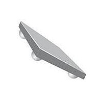
... NXP Semiconductors 10. Package outline WLCSP4: wafer level chip-size package; 4 bumps; 0.91 x 0.91 x 0.65 mm ball A1 index area B A ball A1 1 index area Dimensions Unit max 0.70 0.26 0.37 0.96 mm nom 0.65 0.24 0.32 0.91 min 0.60 0.22 0.27 0.86 Outline version IEC IP4085CX4/LF Fig 20 ...
Page 12
... NXP Semiconductors WLCSP4: wafer level chip-size package; 4 bumps; 0.76 x 0.76 x 0.61 mm ball A1 index area B A ball A1 1 index area Dimensions Unit max 0.66 0.22 0.31 0.81 mm nom 0.61 0.20 0.26 0.76 min 0.56 0.18 0.21 0.71 Outline version IEC IP438xCX4/LF Fig 21. Package outline IP438xCX4/LF (WLCSP4) ...
Page 13
... NXP Semiconductors 11. Design and assembly recommendations 11.1 PCB design guidelines For optimum performance it is recommended to use a Non-Solder Mask PCB Design (NSMD), also known as a copper-defined design, incorporating laser-drilled micro-vias connecting the ground pads to a buried ground-plane layer. This results in the lowest possible ground inductance and provides the best high frequency and ESD performance ...
Page 14
... NXP Semiconductors Table 8. Symbol T reflow(peak dT/dt 12. Abbreviations Table 9. Acronym DUT FR4 LAN PCB PCS RoHS WAN WLCSP 13. Revision history Table 10. Revision history Document ID IP4085_4385_4386_4387_CX4_1 IP4085_4385_4386_4387_CX4_1 Product data sheet IP4085/4385/4386/4387/CX4 Integrated high-performance ESD-protection diodes Reflow soldering process characteristics Parameter Conditions peak reflow temperature ...
Page 15
... Right to make changes — NXP Semiconductors reserves the right to make changes to information published in this document, including without limitation specifications and product descriptions, at any time and without notice ...
Page 16
... NXP Semiconductors 16. Contents 1 Product profi 1.1 General description 1.2 Features . . . . . . . . . . . . . . . . . . . . . . . . . . . . . . 1 1.3 Applications . . . . . . . . . . . . . . . . . . . . . . . . . . . 1 2 Pinning information . . . . . . . . . . . . . . . . . . . . . . 2 3 Ordering information . . . . . . . . . . . . . . . . . . . . . 2 4 Functional diagram . . . . . . . . . . . . . . . . . . . . . . 2 5 Limiting values Thermal characteristics Characteristics . . . . . . . . . . . . . . . . . . . . . . . . . . 4 8 Application information 8.1 Forward current DC clamping voltage . . . . . . . 5 8.2 Peak clamping voltage . . . . . . . . . . . . . . . . . . . 7 9 Marking . . . . . . . . . . . . . . . . . . . . . . . . . . . . . . . 10 10 Package outline ...