ORDERING INFORMATION
GENERAL DESCRIPTION
The ALD1115 is a monolithic complementary N-channel and P-channel
transistor pair intended for a broad range of analog applications. These
enhancement-mode transistors are manufactured with Advanced Linear
Devices' enhanced ACMOS silicon gate CMOS process. It consists of
a N-channel MOSFET and a P-channel MOSFET in one package. The
ALD1115 is a dual version of the quad complementary ALD1105.
The ALD1115 offers high input impedance and negative current
temperature coefficient. The transistor pair is designed for precision
signal switching and amplifying applications in +1V to +12V systems
where low input bias current, low input capacitance and fast switching
speed are desired. Since these are MOSFET devices, they feature very
large (almost infinite) current gain in a low frequency, or near DC,
operating environment. When connected in parallel with sources, drains
and gates connected together, a CMOS analog switch can be constructed.
In addition, the ALD1115 is intended as a building block for CMOS
inverters, differential amplifier input stages, transmission gates, and
multiplexer applications.
The ALD1115 is suitable for use in precision applications which require
very high current gain, beta, such as current mirrors and current sources.
The high input impedance and the high DC current gain of the field effect
transistors result in extremely low current loss through the control gate.
The DC current gain is limited by the gate input leakage current, which
is specified at 30pA at room temperature. V+ is connected to the
substrate, which is the most positive voltage potential of the ALD1115,
usually SP(5). Similarly, V- is connected to the most negative voltage
potential of the ALD1115, usually SN (1).
© 2006 Advanced Linear Devices, Inc. 415 Tasman Drive, Sunnyvale, California 94089 -1706 Tel: (408) 747-1155 Fax: (408) 747-1286 http://www.aldinc.com
FEATURES
• Thermal tracking between N-channel and P-channel
• Low threshold voltage of 0.7V for both N-channel
• Low input capacitance
• High input impedance -- 10
• Low input and output leakage currents
• Negative current (I
• Enhancement mode (normally off)
• DC current gain 10
• Single N-channel MOSFET and single P-channel
* Contact factory for industrial temperature range.
and P-channel MOSFETs
MOSFET in one package
-55 C to +125 C
8-Pin
CERDIP
Package
ALD1115 DA
A
L
D
INEAR
DVANCED
EVICES,
0 C to +70 C
8-Pin
MSOP
Package
ALD1115 MAL
Operating Temperature Range*
DS
9
COMPLEMENTARY N-CHANNEL AND P-CHANNEL MOSFET
I
) temperature coefficient
NC.
("L"suffix for lead free version)
13
typical
0 C to +70 C
8-Pin
Plastic Dip
Package
ALD1115 PA
ALD1115PAL
0 C to +70 C
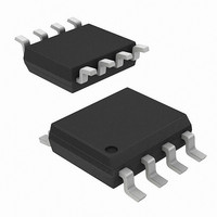
8-Pin
SOIC
Package
ALD1115 SA
ALD1115 SAL
PIN CONFIGURATION
APPLICATIONS
• Precision current mirrors
• Complementary push-pull linear drives
• Discrete analog switches
• Analog signal choppers
• Differential amplifier input stage
• Voltage comparator
• Data converters
• Sample and Hold
• Analog current inverter
• Precision matched current sources
• CMOS inverter stage
• Diode clamps
• Source followers
BLOCK DIAGRAM
GN
SN
DN
V
N DRAIN 1 (3)
P DRAIN 1 (7)
-
4
1
2
3
DA, MA, PA, SA PACKAGE
N GATE 1 (2)
P GATE 1 (6)
N SOURCE 1 (1)
V - (4)
P SOURCE 1 (5)
V + (8)
ALD1115
5
7
6
8
DP
GP
SP
V
+