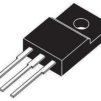
NDF06N62ZG ON Semiconductor, NDF06N62ZG Datasheet - Page 2

NDF06N62ZG
Manufacturer Part Number
NDF06N62ZG
Description
MOSFET N-CH 620V 1.2OHM TO220FP
Manufacturer
ON Semiconductor
Datasheet
1.NDF06N62ZG.pdf
(6 pages)
Specifications of NDF06N62ZG
Fet Type
MOSFET N-Channel, Metal Oxide
Fet Feature
Standard
Rds On (max) @ Id, Vgs
1.2 Ohm @ 3A, 10V
Drain To Source Voltage (vdss)
620V
Current - Continuous Drain (id) @ 25° C
6A
Vgs(th) (max) @ Id
4.5V @ 100µA
Gate Charge (qg) @ Vgs
32nC @ 10V
Input Capacitance (ciss) @ Vds
923pF @ 25V
Power - Max
31W
Mounting Type
Through Hole
Package / Case
TO-220FP
Configuration
Single
Transistor Polarity
N-Channel
Resistance Drain-source Rds (on)
0.98 Ohms
Forward Transconductance Gfs (max / Min)
5 S
Drain-source Breakdown Voltage
620 V
Continuous Drain Current
3.8 A
Power Dissipation
31 W
Maximum Operating Temperature
+ 150 C
Mounting Style
Through Hole
Gate Charge Qg
32 nC
Minimum Operating Temperature
- 55 C
Lead Free Status / RoHS Status
Lead free / RoHS Compliant
Other names
NDF06N62ZG
NDF06N62ZGOS
NDF06N62ZGOS
Available stocks
Company
Part Number
Manufacturer
Quantity
Price
Company:
Part Number:
NDF06N62ZG
Manufacturer:
ON
Quantity:
2 800
3. Insertion mounted
4. Pulse Width ≤ 380 ms, Duty Cycle ≤ 2%.
THERMAL RESISTANCE
ELECTRICAL CHARACTERISTICS
OFF CHARACTERISTICS
ON CHARACTERISTICS (Note 4)
DYNAMIC CHARACTERISTICS
RESISTIVE SWITCHING CHARACTERISTICS
SOURCE−DRAIN DIODE CHARACTERISTICS (T
Junction−to−Case (Drain)
Junction−to−Ambient Steady State (Note 3)
Drain−to−Source Breakdown Voltage
Breakdown Voltage Temperature
Drain−to−Source Leakage Current
Gate−to−Source Forward Leakage
Static Drain−to−Source
Gate Threshold Voltage
Forward Transconductance
Input Capacitance
Output Capacitance
Reverse Transfer Capacitance
Total Gate Charge
Gate−to−Source Charge
Gate−to−Drain (“Miller”) Charge
Plateau Voltage
Gate Resistance
Turn−On Delay Time
Rise Time
Turn−Off Delay Time
Fall Time
Diode Forward Voltage
Reverse Recovery Time
Reverse Recovery Charge
Coefficient
On−Resistance
Characteristic
Parameter
(T
V
J
DS
= 25°C unless otherwise noted)
I
S
= 620 V, V
V
V
V
V
V
V
V
V
= 6.0 A, di/dt = 100 A/ms
V
DD
DD
I
DS
DS
C
S
GS
Reference to 25°C,
GS
DS
GS
GS
Test Conditions
= 6.0 A, V
= 25°C unless otherwise noted)
= 310 V, I
= 310 V, I
= V
= 25 V, V
= 0 V, V
V
= 10 V, I
= 15 V, I
= 10 V, R
f = 1.0 MHz
= 0 V, I
V
I
GS
D
GS
GS
http://onsemi.com
= 1 mA
GS
= ±20 V
, I
= 10 V
D
D
DD
= 0 V
D
D
GS
D
D
GS
= 100 mA
= 1 mA
G
= 3.0 A
= 3.0 A
= 6.0 A,
= 6.0 A,
= 30 V
= 5 Ω
= 0 V
= 0 V,
2
125°C
25°C
DBV
Symbol
Symbol
R
V
BV
R
t
t
R
I
C
I
DS(on)
DT
GS(th)
C
C
V
g
Q
Q
V
d(on)
d(off)
GSS
DSS
Q
Q
R
qJC
qJA
t
oss
t
FS
rss
t
SD
DSS
iss
gp
rr
gs
gd
r
f
DSS
g
g
rr
J
/
NDF06N62Z
Min
620
3.0
4.0
50
0.98
Typ
923
106
338
0.6
5.0
6.3
6.3
3.2
2.0
23
32
17
13
19
32
28
NDP06N62Z
1.1
50
Max
±10
1.2
4.5
1.6
50
1
°C/W
V/°C
Unit
Unit
mA
mA
pF
nC
mC
ns
ns
W
W
V
V
S
V
V


