STW17N62K3 STMicroelectronics, STW17N62K3 Datasheet
STW17N62K3
Specifications of STW17N62K3
Available stocks


Related parts for STW17N62K3


STW17N62K3 Summary of contents
Page 1
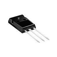
... Table 1. Device summary Order codes STF17N62K3 STP17N62K3 STW17N62K3 November 2008 STP17N62K3, STW17N62K3 SuperMESH3™ Power MOSFET ( TO-247 15 A 190 190 W Figure 1 ...
Page 2
... Electrical characteristics (curves) 3 Test circuits 4 Package mechanical data . . . . . . . . . . . . . . . . . . . . . . . . . . . . . . . . . . . . 10 5 Package mechanical data . . . . . . . . . . . . . . . . . . . . . . . . . . . . . . . . . . . . 15 6 Revision history . . . . . . . . . . . . . . . . . . . . . . . . . . . . . . . . . . . . . . . . . . . 16 2/15 STF17N62K3, STP17N62K3, STW17N62K3 . . . . . . . . . . . . . . . . . . . . . . . . . . . . . . . . . . . . . . . . . . . . . . ...
Page 3
... STF17N62K3, STP17N62K3, STW17N62K3 1 Electrical ratings Table 2. Absolute maximum ratings Symbol V Drain-source voltage ( Gate- source voltage GS I Drain current (continuous Drain current (continuous (2) I Drain current (pulsed Total dissipation at T TOT Derating factor Gate source ESD(HBM-C = 100 pF, V ESD(G- 1.5 kΩ) (3) dv/dt ...
Page 4
... C oss eq increases from 0 to 80% V Table 7. Switching times Symbol Parameter t Turn-on delay time d(on) t Rise time r t Turn-off-delay time d(off) t Fall time f 4/15 STF17N62K3, STP17N62K3, STW17N62K3 Parameter Test conditions mA Max rating Max rating ± ...
Page 5
... STF17N62K3, STP17N62K3, STW17N62K3 Table 8. Source drain diode Symbol I Source-drain current SD (1) I Source-drain current (pulsed) SDM (2) V Forward on voltage SD t Reverse recovery time rr Q Reverse recovery charge rr I Reverse recovery current RRM t Reverse recovery time rr Q Reverse recovery charge rr I Reverse recovery current RRM 1 ...
Page 6
... Figure 6. Safe operating area for TO-247 6/15 STF17N62K3, STP17N62K3, STW17N62K3 Figure 3. AM01479v1 10µs 100µs 1ms 10ms Figure 5. AM01480v1 10µs 100µs 1ms 10ms Figure 7. AM01493v1 10µs 100µs 1ms 10ms Thermal impedance for TO-220 Thermal impedance for TO-220FP ...
Page 7
... STF17N62K3, STP17N62K3, STW17N62K3 Figure 8. Output characteristics Figure 10. Normalized BV V (BR)DSS (norm) 1.10 1.05 1.00 0.95 0.90 0.85 -50 0 Figure 12. Gate charge vs gate-source voltage Figure 13. Capacitance variations V GS (V) V =496V DD I =15A =10V Figure 9. vs temperature Figure 11. Static drain-source on resistance DSS AM01490v1 ...
Page 8
... Figure 14. Normalized gate threshold voltage vs temperature V GS(th) (norm) 1.1 1.0 0.9 0.8 0.7 0 -50 Figure 16. Source-drain diode forward characteristics 8/15 STF17N62K3, STP17N62K3, STW17N62K3 Figure 15. Normalized on resistance vs AM01487v1 R DS(on) (norm) 2.5 2.0 1.5 1.0 0.5 0.0 100 150 T (°C) J Figure 17. Maximum avalanche energy vs ...
Page 9
... STF17N62K3, STP17N62K3, STW17N62K3 3 Test circuits Figure 18. Switching times test circuit for resistive load Figure 20. Test circuit for inductive load switching and diode recovery times Figure 22. Unclamped inductive waveform Figure 19. Gate charge test circuit Figure 21. Unclamped Inductive load test circuit Figure 23. Switching time waveform ...
Page 10
... These packages have a Lead-free second level interconnect. The category of second level interconnect is marked on the package and on the inner box label, in compliance with JEDEC Standard JESD97. The maximum ratings related to soldering conditions are also marked on the inner box label. ECOPACK trademark. ECOPACK specifications are available at: 10/15 STF17N62K3, STP17N62K3, STW17N62K3 www.st.com ...
Page 11
... STF17N62K3, STP17N62K3, STW17N62K3 Dim L20 L30 ∅P Q TO-220 mechanical data mm Min Typ Max 4.40 4.60 0.61 0.88 1.14 1.70 0.48 0.70 15.25 15.75 1.27 10 10.40 2.40 2.70 4.95 5.15 1.23 1.32 6.20 6.60 2.40 2. 3.50 3.93 16.40 28.90 3.75 3.85 2.65 2 ...
Page 12
... Package mechanical data Dim Dia 12/15 STF17N62K3, STP17N62K3, STW17N62K3 TO-220FP mechanical data mm. Min. Typ Max. 4.40 4.60 2.5 2.7 2.5 2.75 0.45 0.70 0.75 1.00 1.15 1.50 1.15 1.50 4.95 5.20 2.40 2.70 10 10.40 16 28.6 30.6 9.80 10.60 2.9 3.6 15.90 16 ...
Page 13
... STF17N62K3, STP17N62K3, STW17N62K3 Dim øP øR S TO-247 Mechanical data mm. Min. Typ 4.85 2.20 1.0 2.0 3.0 0.40 19.85 15.45 5.45 14.20 3.70 18.50 3.55 4.50 5.50 Package mechanical data Max. 5.15 2.60 1.40 2.40 3.40 0.80 20.15 15.75 14.80 4.30 3.65 5 ...
Page 14
... Revision history 5 Revision history Table 10. Document revision history Date 11-Nov-2008 14/15 STF17N62K3, STP17N62K3, STW17N62K3 Revision 1 First release Changes ...
Page 15
... STF17N62K3, STP17N62K3, STW17N62K3 Information in this document is provided solely in connection with ST products. STMicroelectronics NV and its subsidiaries (“ST”) reserve the right to make changes, corrections, modifications or improvements, to this document, and the products and services described herein at any time, without notice. All ST products are sold pursuant to ST’s terms and conditions of sale. ...