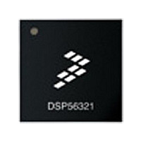
XC56309VL100A Freescale Semiconductor, XC56309VL100A Datasheet - Page 181

XC56309VL100A
Manufacturer Part Number
XC56309VL100A
Description
IC DSP 24BIT 100MHZ 196-MAPBGA
Manufacturer
Freescale Semiconductor
Series
DSP563xxr
Type
Fixed Pointr
Specifications of XC56309VL100A
Interface
Host Interface, SSI, SCI
Clock Rate
100MHz
Non-volatile Memory
ROM (576 B)
On-chip Ram
24kB
Voltage - I/o
3.30V
Voltage - Core
3.30V
Operating Temperature
-40°C ~ 100°C
Mounting Type
Surface Mount
Package / Case
196-MAPBGA
Device Core Size
24b
Format
Fixed Point
Clock Freq (max)
100MHz
Mips
100
Device Input Clock Speed
100MHz
Ram Size
102KB
Operating Supply Voltage (typ)
3.3V
Operating Supply Voltage (min)
3V
Operating Supply Voltage (max)
3.6V
Operating Temp Range
-40C to 100C
Operating Temperature Classification
Industrial
Mounting
Surface Mount
Pin Count
196
Package Type
MA-BGA
Lead Free Status / RoHS Status
Lead free / RoHS Compliant
Available stocks
Company
Part Number
Manufacturer
Quantity
Price
Company:
Part Number:
XC56309VL100A
Manufacturer:
Freescale Semiconductor
Quantity:
10 000
Company:
Part Number:
XC56309VL100AR2
Manufacturer:
Freescale Semiconductor
Quantity:
10 000
- Current page: 181 of 284
- Download datasheet (4Mb)
Freescale Semiconductor
Number
Bit
8
7
6
5
WOMS
WAKE
Name
RWU
RE
Bit
Table 8-2. SCI Control Register (SCR) Bit Definitions (Continued)
Reset
Value
0
0
0
0
Receiver Enable
When RE is set, the receiver is enabled. When RE is cleared, the receiver is disabled,
and data transfer from the receive shift register to the receive data register (SRX) is
inhibited. If RE is cleared while a character is being received, the reception of the
character completes before the receiver is disabled. RE does not inhibit RDRF or receive
interrupts. Either a hardware RESET signal or a software RESET instruction clears RE.
Wired-OR Mode Select
When WOMS is set, the SCI TXD driver is programmed to function as an open-drain
output and can be wired together with other TXD signals in an appropriate bus
configuration, such as a master-slave multidrop configuration. An external pullup resistor
is required on the bus. When WOMS is cleared, the TXD signal uses an active internal
pullup. Either a hardware RESET signal or a software RESET instruction clears WOMS.
Receiver Wakeup Enable
When RWU is set and the SCI is in Asynchronous mode, the wakeup function is enabled;
that is, the SCI is asleep and can be awakened by the event defined by the WAKE bit. In
Sleep state, all interrupts and all receive flags except IDLE are disabled. When the
receiver wakes up, RWU is cleared by the wakeup hardware. You can also clear the
RWU bit to wake up the receiver. You can use RWU to ignore messages that are for
other devices on a multidrop serial network. Wakeup on idle line (i. e., WAKE is cleared)
or wakeup on address bit (i. e., WAKE is set) must be chosen. When WAKE is cleared
and RWU is set, the receiver does not respond to data on the data line until an idle line is
detected. When WAKE is set and RWU is set, the receiver does not respond to data on
the data line until a data frame with Bit 9 set is detected.
When the receiver wakes up, the RWU bit is cleared, and the first frame of data is
received. If interrupts are enabled, the CPU is interrupted and the interrupt routine reads
the message header to determine whether the message is intended for this DSP. If the
message is for this DSP, the message is received, and RWU is set to wait for the next
message. If the message is not for this DSP, the DSP immediately sets RWU. Setting
RWU causes the DSP to ignore the remainder of the message and wait for the next
message. Either a hardware RESET signal or a software RESET instruction clears RWU.
RWU is ignored in Synchronous mode.
Wakeup Mode Select
When WAKE is cleared, the wakeup on Idle Line mode is selected. In the wakeup on idle
line mode, the SCI receiver is re-enabled by an idle string of at least 10 or 11 (depending
on WDS mode) consecutive ones. The transmitter’s software must provide this idle string
between consecutive messages. The idle string cannot occur within a valid message
because each word frame there contains a start bit that is 0.
When WAKE is set, the wakeup on address bit mode is selected. In the wakeup on
address bit mode, the SCI receiver is re-enabled when the last (eighth or ninth) data bit
received in a character (frame) is 1. The ninth data bit is the address bit (R8) in the 11-bit
multidrop mode; the eighth data bit is the address bit in the 10-bit asynchronous and
11-bit asynchronous with parity modes. Thus, the received character is an address that
has to be processed by all sleeping processors—that is, each processor has to compare
the received character with its own address and decide whether to receive or ignore all
following characters.
DSP56309 User’s Manual, Rev. 1
Description
SCI Programming Model
8-13
Related parts for XC56309VL100A
Image
Part Number
Description
Manufacturer
Datasheet
Request
R
Part Number:
Description:
Manufacturer:
Freescale Semiconductor, Inc
Datasheet:
Part Number:
Description:
Manufacturer:
Freescale Semiconductor, Inc
Datasheet:
Part Number:
Description:
Manufacturer:
Freescale Semiconductor, Inc
Datasheet:
Part Number:
Description:
Manufacturer:
Freescale Semiconductor, Inc
Datasheet:
Part Number:
Description:
Manufacturer:
Freescale Semiconductor, Inc
Datasheet:
Part Number:
Description:
Manufacturer:
Freescale Semiconductor, Inc
Datasheet:
Part Number:
Description:
Manufacturer:
Freescale Semiconductor, Inc
Datasheet:
Part Number:
Description:
Manufacturer:
Freescale Semiconductor, Inc
Datasheet:
Part Number:
Description:
Manufacturer:
Freescale Semiconductor, Inc
Datasheet:
Part Number:
Description:
Manufacturer:
Freescale Semiconductor, Inc
Datasheet:
Part Number:
Description:
Manufacturer:
Freescale Semiconductor, Inc
Datasheet:
Part Number:
Description:
Manufacturer:
Freescale Semiconductor, Inc
Datasheet:
Part Number:
Description:
Manufacturer:
Freescale Semiconductor, Inc
Datasheet:
Part Number:
Description:
Manufacturer:
Freescale Semiconductor, Inc
Datasheet:
Part Number:
Description:
Manufacturer:
Freescale Semiconductor, Inc
Datasheet:


