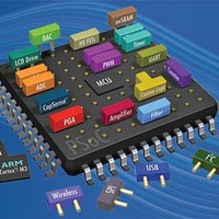
CY8C3866PVI-070 Cypress Semiconductor Corp, CY8C3866PVI-070 Datasheet - Page 36

CY8C3866PVI-070
Manufacturer Part Number
CY8C3866PVI-070
Description
IC MCU 8BIT 64KB FLASH 48SSOP
Manufacturer
Cypress Semiconductor Corp
Series
PSOC™ 3 CY8C38xxr
Specifications of CY8C3866PVI-070
Package / Case
*
Voltage - Supply (vcc/vdd)
1.71 V ~ 5.5 V
Operating Temperature
-40°C ~ 85°C
Speed
67MHz
Number Of I /o
25
Eeprom Size
2K x 8
Core Processor
8051
Program Memory Type
FLASH
Ram Size
8K x 8
Program Memory Size
64KB (64K x 8)
Data Converters
A/D 2x20b, D/A 4x8b
Oscillator Type
Internal
Peripherals
CapSense, DMA, LCD, POR, PWM, WDT
Connectivity
CAN, EBI/EMI, I²C, LIN, SPI, UART/USART
Core Size
8-Bit
Operating Temperature (min)
-40C
Operating Temperature (max)
85C
Technology
CMOS
Processing Unit
Microcontroller
Operating Supply Voltage (min)
1.8V
Operating Supply Voltage (typ)
2.5/3.3/5V
Operating Supply Voltage (max)
5.5V
Package Type
SSOP
Screening Level
Industrial
Pin Count
48
Mounting
Surface Mount
Rad Hardened
No
Processor Series
CY8C38
Core
8051
Data Bus Width
32 bit
Data Ram Size
8 KB
Interface Type
I2C, SPI, UART, USB
Maximum Clock Frequency
67 MHz
Number Of Programmable I/os
28 to 72
Number Of Timers
4
Operating Supply Voltage
0.5 V to 5.5 V
Maximum Operating Temperature
+ 85 C
Mounting Style
SMD/SMT
Controller Family/series
(8051) PSOC 3
No. Of I/o's
25
Eeprom Memory Size
2KB
Ram Memory Size
8KB
Cpu Speed
67MHz
Rohs Compliant
Yes
Lead Free Status / RoHS Status
Lead free / RoHS Compliant
Lead Free Status / RoHS Status
Compliant, Lead free / RoHS Compliant
Available stocks
Company
Part Number
Manufacturer
Quantity
Price
Part Number:
CY8C3866PVI-070
Manufacturer:
CYPRESS厂技术支持
Quantity:
20 000
6.4.1 Drive Modes
Each GPIO and SIO pin is individually configurable into one of the eight drive modes listed in
used for each pin (DM[2:0]) and set in the PRTxDM[2:0] registers.
drive modes.
selected. Note that the actual I/O pin voltage is determined by a combination of the selected drive mode and the load at the pin. For
example, if a GPIO pin is configured for resistive pull-up mode and driven high while the pin is floating, the voltage measured at the
pin is a high logic state. If the same GPIO pin is externally tied to ground then the voltage unmeasured at the pin is a low logic state.
Table 6-6. Drive Modes
Document Number: 001-11729 Rev. *R
Note
15. Resistive pull-up and pull-down are not available with SIO in regulated output mode.
Diagram
0
1
2
3
4
5
6
7
Table 6-6
High impedence analog
High Impedance digital
Resistive pull-up
Resistive pull-down
Open drain, drives low
Open drain, drive high
Strong drive
Resistive pull-up and pull-down
shows the I/O pin’s drive state based on the port data register value or digital array signal if bypass mode is
Drive Mode
0.
4.
DR
PS
DR
PS
[15]
Open Drain ,
Drives Low
High Impedance
Analog
[15]
Pin
Pin
[15]
1.
PS
5.
DR
DR
PS
Open Drain ,
Drives High
High Impedance
Digital
Figure 6-11. Drive Mode
PRTxDM2
Vddio
0
0
0
0
1
1
1
1
Pin
Pin
2.
6.
DR
PS
DR
PS
Figure 6-11
Strong Drive
Resistive
Pull-Up
PRTxDM1
Vddio
Vddio
0
0
1
1
0
0
1
1
Pin
Pin
depicts a simplified pin view based on each of the eight
3.
7.
DR
PS
DR
PS
PRTxDM0
Resistive
Pull-Up and Pull-Down
Resistive
Pull-Down
0
1
0
1
0
1
0
1
Vddio
Vddio
PSoC
Pin
Pin
Table
Res High (5K)
Res High (5K)
PRTxDR = 1
Strong High
Strong High
Strong High
®
6-6. Three configuration bits are
High Z
High Z
High Z
3: CY8C38 Family
Data Sheet
Res Low (5K)
Res Low (5K)
PRTxDR = 0
Page 36 of 129
Strong Low
Strong Low
Strong Low
High Z
High Z
High Z
[+] Feedback


