ST16C2552IJ44-F Exar Corporation, ST16C2552IJ44-F Datasheet - Page 24
ST16C2552IJ44-F
Manufacturer Part Number
ST16C2552IJ44-F
Description
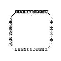
IC UART FIFO 16B DUAL 44PLCC
Manufacturer
Exar Corporation
Type
RS- 232 or RS- 485r
Specifications of ST16C2552IJ44-F
Number Of Channels
2, DUART
Package / Case
44-LCC (J-Lead)
Features
*
Fifo's
16 Byte
Protocol
RS232, RS485
Voltage - Supply
3.3 V ~ 5 V
With False Start Bit Detection
Yes
With Modem Control
Yes
With Cmos
Yes
Mounting Type
Surface Mount
Data Rate
4 Mbps
Supply Voltage (max)
5.5 V
Supply Voltage (min)
2.97 V
Supply Current
3 mA
Maximum Operating Temperature
+ 85 C
Minimum Operating Temperature
- 40 C
Mounting Style
SMD/SMT
Operating Supply Voltage
3.3 V or 5 V
No. Of Channels
2
Supply Voltage Range
2.97V To 5.5V
Operating Temperature Range
-40°C To +85°C
Digital Ic Case Style
PLCC
No. Of Pins
44
Filter Terminals
SMD
Rohs Compliant
Yes
Lead Free Status / RoHS Status
Lead free / RoHS Compliant
Lead Free Status / RoHS Status
Lead free / RoHS Compliant, Lead free / RoHS Compliant
Other names
1016-1258-5
Available stocks
Company
Part Number
Manufacturer
Quantity
Price
Company:

Part Number:
ST16C2552IJ44-F
Manufacturer:
Exar Corporation
Quantity:
135
Company:
Part Number:
ST16C2552IJ44-F
Manufacturer:
IDT
Quantity:
4 795
Company:
Part Number:
ST16C2552IJ44-F
Manufacturer:
Exar Corporation
Quantity:
10 000


ST16C2552
2.97V TO 5.5V DUAL UART WITH 16-BYTE FIFO
MSR[7]: CD Input Status
Normally this bit is the compliment of the CD# input. In the loopback mode this bit is equivalent to bit-3 in the
MCR register. The CD# input may be used as a general purpose input when the modem interface is not used.
This is a 8-bit general purpose register for the user to store temporary data. The content of this register is
preserved during sleep mode but becomes 0xFF (default) after a reset or a power off-on cycle.
The concatenation of the contents of DLM and DLL gives the 16-bit divisor value which is used to calculate the
baud rate:
•
See MCR bit-7 and the baud rate table also.
This register is used to select specific modes of MF# operation and to allow both UART register sets to be
written concurrently.
AFR[0]: Concurrent Write Mode
When this bit is set, the CPU can write concurrently to the same register in both UARTs. This function is
intended to reduce the dual UART initialization time. It can be used by the CPU when both channels are
initialized to the same state. The external CPU can set or clear this bit by accessing either register set. When
this bit is set, the channel select pin still selects the channel to be accessed during read operations. The user
should ensure that LCR Bit-7 of both channels are in the same state before executing a concurrent write to the
registers at address 0, 1, or 2.
•
•
AFR[2:1]: MF# Output Select
These bits select a signal function for output on the MF# A/B pins. These signal function are described as:
OP2#, BAUDOUT#, or RXRDY#. Only one signal function can be selected at a time.
AFR[7:3]: Reserved
All are initialized to logic 0.
4.11
4.12
4.13
Baud Rate = (Clock Frequency / 16) / Divisor
Logic 0 = No concurrent write (default).
Logic 1 = Register set A and B are written concurrently with a single external CPU I/O write operation.
Scratch Pad Register (SPR) - Read/Write
Baud Rate Generator Registers (DLL and DLM) - Read/Write
Alternate Function Register (AFR) - Read/Write
B
IT
0
0
1
1
-2
B
IT
0
1
0
1
-1
24
MF# F
OP2# (default)
BAUDOUT#
Reserved
RXRDY#
UNCTION
REV. 4.2.2
Related parts for ST16C2552IJ44-F
Image
Part Number
Description
Manufacturer
Datasheet
Request
R

Part Number:
Description:
2.97V TO 5.5V DUAL UART WITH 16-BYTE FIFO
Manufacturer:
Exar Corporation
Part Number:
Description:
BiCMOS Fixed, Quad, Voltage Output, Single or Dual Supply 8-Bit Digital-to-Analog Converter
Manufacturer:
Exar Corporation
Datasheet:
Part Number:
Description:
Manufacturer:
Exar Corporation
Datasheet:
Part Number:
Description:
Voltage-Controlled Oscillator
Manufacturer:
Exar Corporation
Datasheet:
Part Number:
Description:
INTEGRATED LINE TRANSMITTER
Manufacturer:
Exar Corporation
Datasheet:
Part Number:
Description:
Monolithic Function Generator
Manufacturer:
Exar Corporation
Datasheet:
Part Number:
Description:
CMOS Microprocessor Compatible Double-Buffered 12-Bit Digital-to-Analog Converter
Manufacturer:
Exar Corporation
Datasheet:
Part Number:
Description:
CMOS 6 BIT HIGH SPEED ANALOG TO DIGITAL CONVERTER
Manufacturer:
Exar Corporation
Datasheet:
Part Number:
Description:
Manufacturer:
Exar Corporation
Datasheet:
Part Number:
Description:
Manufacturer:
Exar Corporation
Datasheet:
Part Number:
Description:
8-Channel, Voltage Output 10 MHz Input Bandwidth 8-Bit Multiplying DACs with Serial Digital Data Por
Manufacturer:
Exar Corporation
Datasheet:
Part Number:
Description:
15 V CMOS Multiplying10-Bit Digital-to-Analog Converter
Manufacturer:
Exar Corporation
Datasheet:
Part Number:
Description:
Monolithic Function Generator
Manufacturer:
Exar Corporation
Datasheet: