ST16C2552IJ44-F Exar Corporation, ST16C2552IJ44-F Datasheet - Page 4
ST16C2552IJ44-F
Manufacturer Part Number
ST16C2552IJ44-F
Description
IC UART FIFO 16B DUAL 44PLCC
Manufacturer
Exar Corporation
Type
RS- 232 or RS- 485r
Specifications of ST16C2552IJ44-F
Number Of Channels
2, DUART
Package / Case
44-LCC (J-Lead)
Features
*
Fifo's
16 Byte
Protocol
RS232, RS485
Voltage - Supply
3.3 V ~ 5 V
With False Start Bit Detection
Yes
With Modem Control
Yes
With Cmos
Yes
Mounting Type
Surface Mount
Data Rate
4 Mbps
Supply Voltage (max)
5.5 V
Supply Voltage (min)
2.97 V
Supply Current
3 mA
Maximum Operating Temperature
+ 85 C
Minimum Operating Temperature
- 40 C
Mounting Style
SMD/SMT
Operating Supply Voltage
3.3 V or 5 V
No. Of Channels
2
Supply Voltage Range
2.97V To 5.5V
Operating Temperature Range
-40°C To +85°C
Digital Ic Case Style
PLCC
No. Of Pins
44
Filter Terminals
SMD
Rohs Compliant
Yes
Lead Free Status / RoHS Status
Lead free / RoHS Compliant
Lead Free Status / RoHS Status
Lead free / RoHS Compliant, Lead free / RoHS Compliant
Other names
1016-1258-5
Available stocks
Company
Part Number
Manufacturer
Quantity
Price
Company:

Part Number:
ST16C2552IJ44-F
Manufacturer:
Exar Corporation
Quantity:
135
Company:
Part Number:
ST16C2552IJ44-F
Manufacturer:
IDT
Quantity:
4 795
Company:
Part Number:
ST16C2552IJ44-F
Manufacturer:
Exar Corporation
Quantity:
10 000


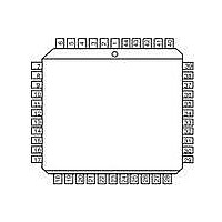
ST16C2552
2.97V TO 5.5V DUAL UART WITH 16-BYTE FIFO
Pin Description
DSRA#
RTSA#
CTSA#
DTRA#
MFA#
MFB#
CDA#
N
TXA
RXA
AME
44-PLCC
P
35
19
38
39
36
40
37
41
42
IN
#
T
YPE
O
O
O
O
O
I
I
I
I
Multi-Function Output Channel A. This output pin can function as the OP2A#, BAUD-
OUTA#, or RXRDYA# pin. One of these output signal functions can be selected by
the user programmable bits 1-2 of the Alternate Function Register (AFR). These sig-
nal functions are described as follows:
1) OP2A# - When OP2A# (active low) is selected, the MF# pin is a logic 0 when MCR
bit-3 is set to a logic 1 (see MCR bit-3). MCR bit-3 defaults to a logic 1 condition after
a reset or power-up.
2) BAUDOUTA# - When BAUDOUTA# function is selected, the 16X Baud rate clock
output is available at this pin.
3) RXRDYA# - RXRDYA# (active low) is intended for monitoring DMA data transfers.
See
If it is not used, leave it unconnected.
Multi-Function Output ChannelB. This output pin can function as the OP2B#, BAUD-
OUTB#, or RXRDYB# pin. One of these output signal functions can be selected by
the user programmable bits 1-2 of the Alternate Function Register (AFR). These sig-
nal functions are described as follows:
1) OP2B# - When OP2B# (active low) is selected, the MF# pin is a logic 0 when MCR
bit-3 is set to a logic 1 (see MCR bit-3). MCR bit-3 defaults to a logic 1 condition after
a reset or power-up.
2) BAUDOUTB# - When BAUDOUTB# function is selected, the 16X Baud rate clock
output is available at this pin.
3) RXRDYB# - RXRDYB# (active low) is intended for monitoring DMA data transfers.
See
If it is not used, leave it unconnected.
UART channel A Transmit Data. If it is not used, leave it unconnected.
UART channel A Receive Data. Normal receive data input must idle at logic 1 condi-
tion. If it is not used, tie it to VCC or pull it high via a 100k ohm resistor.
UART channel A Request-to-Send (active low) or general purpose output. If it is not
used, leave it unconnected.
UART channel A Clear-to-Send (active low) or general purpose input. This input
should be connected to VCC when not used. This input has no effect on the UART.
UART channel A Data-Terminal-Ready (active low) or general purpose output. If it is
not used, leave it unconnected.
UART channel A Data-Set-Ready (active low) or general purpose input. This input
should be connected to VCC when not used. This input has no effect on the UART.
UART channel A Carrier-Detect (active low) or general purpose input. This input
should be connected to VCC when not used. This input has no effect on the UART.
Table 2
Table 2
for more details.
for more details.
4
D
ESCRIPTION
REV. 4.2.2
Related parts for ST16C2552IJ44-F
Image
Part Number
Description
Manufacturer
Datasheet
Request
R

Part Number:
Description:
2.97V TO 5.5V DUAL UART WITH 16-BYTE FIFO
Manufacturer:
Exar Corporation
Part Number:
Description:
BiCMOS Fixed, Quad, Voltage Output, Single or Dual Supply 8-Bit Digital-to-Analog Converter
Manufacturer:
Exar Corporation
Datasheet:
Part Number:
Description:
Manufacturer:
Exar Corporation
Datasheet:
Part Number:
Description:
Voltage-Controlled Oscillator
Manufacturer:
Exar Corporation
Datasheet:
Part Number:
Description:
INTEGRATED LINE TRANSMITTER
Manufacturer:
Exar Corporation
Datasheet:
Part Number:
Description:
Monolithic Function Generator
Manufacturer:
Exar Corporation
Datasheet:
Part Number:
Description:
CMOS Microprocessor Compatible Double-Buffered 12-Bit Digital-to-Analog Converter
Manufacturer:
Exar Corporation
Datasheet:
Part Number:
Description:
CMOS 6 BIT HIGH SPEED ANALOG TO DIGITAL CONVERTER
Manufacturer:
Exar Corporation
Datasheet:
Part Number:
Description:
Manufacturer:
Exar Corporation
Datasheet:
Part Number:
Description:
Manufacturer:
Exar Corporation
Datasheet:
Part Number:
Description:
8-Channel, Voltage Output 10 MHz Input Bandwidth 8-Bit Multiplying DACs with Serial Digital Data Por
Manufacturer:
Exar Corporation
Datasheet:
Part Number:
Description:
15 V CMOS Multiplying10-Bit Digital-to-Analog Converter
Manufacturer:
Exar Corporation
Datasheet:
Part Number:
Description:
Monolithic Function Generator
Manufacturer:
Exar Corporation
Datasheet: