TDA9801/V1,112 NXP Semiconductors, TDA9801/V1,112 Datasheet - Page 13
TDA9801/V1,112
Manufacturer Part Number
TDA9801/V1,112
Description
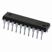
IC PLL DEMODULATOR 20-DIP
Manufacturer
NXP Semiconductors
Datasheet
1.TDA9801V1112.pdf
(32 pages)
Specifications of TDA9801/V1,112
Package / Case
20-DIP (0.300", 7.62mm)
Function
Demodulator, Detector
Current - Supply
70mA
Voltage - Supply
4.5 V ~ 9.9 V
Mounting Style
Through Hole
Lead Free Status / RoHS Status
Lead free / RoHS Compliant
Gain
-
Noise Figure
-
P1db
-
Lo Frequency
-
Rf Frequency
-
Lead Free Status / RoHS Status
Lead free / RoHS Compliant, Lead free / RoHS Compliant
Other names
935260644112
TDA9801N
TDA9801N
TDA9801N
TDA9801N


Philips Semiconductors
Notes
1. Values of video and sound parameters can be decreased at V
2. This parameter is not tested during production and is only given as application information for designing the television
3. Conditions for video demodulator:
4. Temperature coefficient of the external LC circuit is equal to zero.
5. V
6. V
7. Broadband transformer at the VIF input (see Fig.12). The C/N ratio at the VIF input for ‘lock-in’ is defined as the VIF
8. The offset current is measured between pin TPLL and half of the supply voltage (V
9. The intercarrier output signal is superimposed to the video signal at pin VSO and can be calculated by the following
1999 Aug 26
Measurements from VIF input to AF output; notes 20 and 21; see Fig.13
S/N
Single standard VIF-PLL demodulator
and FM-PLL detector
SYMBOL
receiver.
a) Loop bandwidth: BL = 60 kHz, natural frequency f
b) Resonance circuit of VCO: Q
input signal (RMS value of sync pulse level) related to a superimposed 5 MHz band-limited white noise signal
(RMS value). The video modulation is for white picture.
a) no input signal at VIF inputs
b) IF amplifier gain at minimum (V
formula:
where
a) 1.0 V (p-p) = video output signal as reference
b)
c)
d) 6 dB = correction term of internal circuitry
e)
f) Example for SAW filter G1962:
V
W
i(VIF)(rms)
i(VIF)
o(intc)(rms)
FPLL input level
voltage is approximately 2.6 V at V
sound shelf value = 20 dB,
---------- -
2 2
V
-------------- - (dB)
V
V
-------------- -
V
2 dB = tolerance of video output and intercarrier output amplitude V
1
i(SC)
i(PC)
i(SC)
i(PC)
signal for nominal video signal.
= correction term for RMS value
= 10 mV; f = 1 MHz (VCO frequency offset related to f
=
=
–
1.0 V (p-p)
27 dB
weighted signal-to-noise
ratio
= sound-to-picture carrier ratio at VIF inputs in dB
PARAMETER
V
o(intc)(rms)
---------- -
2 2
1
o
10
> 50, see Table 2 for the value of the external capacitor C; C
=
AGC
32 mV (typical value)
V
-------------- - (dB)
------------------------------------------------------------------
V
i(SC)
i(PC)
P
= V
= 5 V and approximately 2.7 V at V
P
) and pin ADJ is left open-circuit.
“CCIR 468-4”
20
+
black picture (sync only) 46
white picture
colour bar
6 dB 2 dB
CONDITIONS
n
= 15 kHz, damping factor d = 2, calculated with grey level and
13
P
= 4.5 V.
PC
); white picture video modulation.
o(intc)(rms)
42
40
MIN.
P
= 9 V.
.
P
52
48
46
= 2.5 V) under the conditions:
TYP.
Product specification
VCO
MAX.
TDA9801
= 8.5 pF, loop
dB
dB
dB
UNIT
Related parts for TDA9801/V1,112
Image
Part Number
Description
Manufacturer
Datasheet
Request
R

Part Number:
Description:
Manufacturer:
NXP Semiconductors
Datasheet:

Part Number:
Description:
RF Wireless Misc VIF-PLL DEM./FM-PLL DET.
Manufacturer:
NXP Semiconductors
Datasheet:
Part Number:
Description:
NXP Semiconductors designed the LPC2420/2460 microcontroller around a 16-bit/32-bitARM7TDMI-S CPU core with real-time debug interfaces that include both JTAG andembedded trace
Manufacturer:
NXP Semiconductors
Datasheet:

Part Number:
Description:
NXP Semiconductors designed the LPC2458 microcontroller around a 16-bit/32-bitARM7TDMI-S CPU core with real-time debug interfaces that include both JTAG andembedded trace
Manufacturer:
NXP Semiconductors
Datasheet:
Part Number:
Description:
NXP Semiconductors designed the LPC2468 microcontroller around a 16-bit/32-bitARM7TDMI-S CPU core with real-time debug interfaces that include both JTAG andembedded trace
Manufacturer:
NXP Semiconductors
Datasheet:
Part Number:
Description:
NXP Semiconductors designed the LPC2470 microcontroller, powered by theARM7TDMI-S core, to be a highly integrated microcontroller for a wide range ofapplications that require advanced communications and high quality graphic displays
Manufacturer:
NXP Semiconductors
Datasheet:
Part Number:
Description:
NXP Semiconductors designed the LPC2478 microcontroller, powered by theARM7TDMI-S core, to be a highly integrated microcontroller for a wide range ofapplications that require advanced communications and high quality graphic displays
Manufacturer:
NXP Semiconductors
Datasheet:
Part Number:
Description:
The Philips Semiconductors XA (eXtended Architecture) family of 16-bit single-chip microcontrollers is powerful enough to easily handle the requirements of high performance embedded applications, yet inexpensive enough to compete in the market for hi
Manufacturer:
NXP Semiconductors
Datasheet:
Part Number:
Description:
The XA-S3 device is a member of Philips Semiconductors? XA(eXtended Architecture) family of high performance 16-bitsingle-chip microcontrollers
Manufacturer:
NXP Semiconductors
Datasheet:

Part Number:
Description:
The NXP BlueStreak LH75401/LH75411 family consists of two low-cost 16/32-bit System-on-Chip (SoC) devices
Manufacturer:
NXP Semiconductors
Datasheet:
Part Number:
Description:
The NXP LPC3130/3131 combine an 180 MHz ARM926EJ-S CPU core, high-speed USB2
Manufacturer:
NXP Semiconductors
Datasheet:
Part Number:
Description:
The NXP LPC3141 combine a 270 MHz ARM926EJ-S CPU core, High-speed USB 2
Manufacturer:
NXP Semiconductors
Part Number:
Description:
The NXP LPC3143 combine a 270 MHz ARM926EJ-S CPU core, High-speed USB 2
Manufacturer:
NXP Semiconductors

Part Number:
Description:
The NXP LPC3152 combines an 180 MHz ARM926EJ-S CPU core, High-speed USB 2
Manufacturer:
NXP Semiconductors