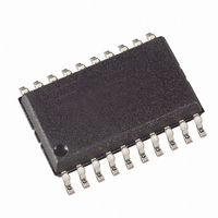
ATA5743P6-TGQY Atmel, ATA5743P6-TGQY Datasheet - Page 14

ATA5743P6-TGQY
Manufacturer Part Number
ATA5743P6-TGQY
Description
IC RCVR ASK/FSK 600KHZ 20SOIC
Manufacturer
Atmel
Datasheet
1.ATA5743P3-TGQY.pdf
(43 pages)
Specifications of ATA5743P6-TGQY
Frequency
300MHz ~ 450MHz
Sensitivity
-110dBm
Data Rate - Maximum
10 kBaud
Modulation Or Protocol
ASK, FSK
Applications
RKE, Telemetering, Security Technology
Current - Receiving
7.5mA
Data Interface
PCB, Surface Mount
Antenna Connector
PCB, Surface Mount
Voltage - Supply
4.5 V ~ 5.5 V
Operating Temperature
-40°C ~ 105°C
Package / Case
20-SOIC (0.300", 7.50mm Width)
Operating Frequency (max)
450000kHz
Operating Temperature (min)
-40C
Operating Temperature (max)
105C
Operating Temperature Classification
Industrial
Operating Supply Voltage (min)
4.5V
Operating Supply Voltage (typ)
5V
Operating Supply Voltage (max)
5.5V
Lead Free Status / RoHS Status
Lead free / RoHS Compliant
Features
-
Memory Size
-
Lead Free Status / Rohs Status
Compliant
Available stocks
Company
Part Number
Manufacturer
Quantity
Price
Company:
Part Number:
ATA5743P6-TGQY
Manufacturer:
ATMEL
Quantity:
222
Part Number:
ATA5743P6-TGQY
Manufacturer:
ATMEL/爱特梅尔
Quantity:
20 000
Figure 6-3.
6.3.1
6.3.2
14
IC_ACTIVE
Bit check
Dem_out
Data_out (DATA)
(Number of checked Bits: 3)
ATA5743
Bit-check Mode
Configuring the Bit Check
Timing Diagram for Complete Successful Bit Check
Start-up mode
In bit-check mode the incoming data stream is examined to distinguish between a valid signal
from a corresponding transmitter, and signals due to noise. This is done by subsequent time
frame checks where the distances between two signal edges are continuously compared to a
programmable time window. The maximum count of this edge-to-edge test before the receiver
switches to receiving mode is also programmable.
Assuming a modulation scheme that contains two edges per bit, two time frame checks verify
one bit. This is valid for Manchester, Bi-phase, and most other modulation schemes. The maxi-
mum count of bits to be checked can be set to 0, 3, 6 or 9 bits via the variable N
OPMODE register. This implies 0, 6, 12 and 18 edge-to-edge checks, respectively. If N
set to a higher value, the receiver is less likely to switch to receiving mode due to noise. In the
presence of a valid transmitter signal, the bit check takes less time if N
value. In polling mode, the bit-check time is not dependent on N
example where 3 bits are tested successfully and the data signal is transferred to pin DATA.
As demonstrated in
limits. If the edge-to-edge time t
bit-check limit, T
T
Figure 6-4.
For best noise immunity it is recommended to use a low span between T
This is achieved by using a fixed frequency at a 50% duty cycle for the transmitter preburst. For
this reason, a “11111...” or a “10101...” sequence in Manchester or Bi-phase is a good choice. A
good compromise between receiver sensitivity and susceptibility to noise is a time window of
±25% regarding the expected edge-to-edge time t
various edge-to-edge time periods, the bit-check limits must be programmed according to the
required span.
T
Lim_max
Start-up
, the bit check will be terminated and the receiver will switch to sleep mode.
Valid Time Window for Bit Check
Lim_max
Figure
1/2 Bit
Dem_out
, the check will be continued. If t
6-4, the time window for the bit check is defined by two separate time
1/2 Bit
Bit-check mode
ee
T
Bit-check
is between the lower bit-check limit, T
1/2 Bit
T
Lim_min
T
Lim_max
t
Bit check ok
ee
1/2 Bit
1/f
Sig
1/2 Bit
ee
ee
. Using preburst patterns that contain
is smaller than T
1/2 Bit
Bit-check
Receiving mode
Bit-check
.
Lim_min
Lim_min
Figure 6-3
Lim_min
is set to a lower
, and the upper
, or t
4839B–RKE–08/05
and T
Bit-check
ee
shows an
Bit-check
exceeds
Lim_max
in the
is
.


