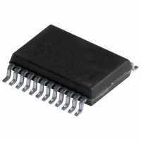
UAA3220TS/V1,118 NXP Semiconductors, UAA3220TS/V1,118 Datasheet - Page 5

UAA3220TS/V1,118
Manufacturer Part Number
UAA3220TS/V1,118
Description
IC RECEIVER ASK/FSK 24SSOP
Manufacturer
NXP Semiconductors
Type
Receiverr
Datasheet
1.UAA3220TSV1118.pdf
(32 pages)
Specifications of UAA3220TS/V1,118
Package / Case
24-SSOP
Frequency
250MHz ~ 920MHz
Sensitivity
-119dBm
Modulation Or Protocol
ASK, FSK
Applications
Car Alarm Systems, RKE
Current - Receiving
4.3mA
Data Interface
PCB, Surface Mount
Antenna Connector
PCB, Surface Mount
Voltage - Supply
2.7 V ~ 5.5 V
Operating Temperature
-40°C ~ 85°C
Operating Frequency
290 MHz
Operating Supply Voltage
3.3 V or 5 V
Maximum Operating Temperature
+ 85 C
Minimum Operating Temperature
- 40 C
Mounting Style
SMD/SMT
Lead Free Status / RoHS Status
Lead free / RoHS Compliant
Features
-
Memory Size
-
Data Rate - Maximum
-
Lead Free Status / Rohs Status
Lead free / RoHS Compliant
Other names
935261031118
UAA3220TSDB-T
UAA3220TSDB-T
UAA3220TSDB-T
UAA3220TSDB-T
Philips Semiconductors
FUNCTIONAL DESCRIPTION
Mixer
The mixer is a single-balanced emitter-coupled mixer with
internal biasing. Matching of the RF source impedance to
the mixer input requires an external matching network.
Oscillator
The oscillator is based on a transistor connected in
common collector configuration followed by a cascode
stage driving a tuned circuit. The voltage at this tuned
circuit drives the frequency multiplier. The bias current of
the oscillator is set by an off-chip resistor (R40 in the
application diagram of Fig.9) to a typical value of 260 A at
433.92 MHz (R40 = 1.8 k ). The oscillator frequency is
controlled by an off-chip overtone crystal (X40). Off-chip
capacitors between base and emitter (C42) and ground
(C41) make the oscillator transistor appear as having
negative resistance at small signal levels. This causes the
oscillator to start. A parallel resonance circuit (L40 and
C41) connected to the emitter of the oscillator transistor
prevents oscillation at the fundamental frequency of the
crystal. The LC tank circuit at the output of the oscillator is
used to select either the fundamental, the second or the
third harmonic of the oscillator frequency.
Frequency multiplier
The frequency multiplier is an emitter-coupled transistor
pair driving an off-chip balanced tuned circuit. The bias
current of this emitter coupled pair is set by an off-chip
resistor (R50) to a typical value of 350 A at 433.92 MHz
(R50 = 1.2 k ). The oscillator output signal is AC-coupled
to one of the inputs of the emitter-coupled pair. The other
input is connected to ground via an on-chip capacitor.
The output voltage of the frequency multiplier drives the
switching stage of the mixer. The bias voltage at this point
is set by an off-chip resistor (R51) to allow sufficient
voltage swing at the mixer outputs.
Post mixer amplifier
The Post Mixer Amplifier (PMA) is a differential input,
single-ended output amplifier. Amplifier gain is provided in
order to reduce the influence of the limiter noise figure on
the total noise figure.
1999 Jan 22
Frequency Shift Keying (FSK)/Amplitude
Shift Keying (ASK) receiver
5
Limiter
The limiter is a single-ended input multiple stage amplifier
with high total gain. Amplifier stability is achieved by
means of an external DC feedback capacitor (C21), which
is also used to determine the lower limiter cut-off
frequency. An RSSI signal proportional to the limiter input
signal is provided. Figure 3 shows the DC voltage at pin 18
(RSSI) as a function of the input voltage (RMS value) at
pin 20 (LIN). It also gives the typical IF of 10.7 MHz.
The lower knee of the level curve (see Fig.3) is determined
by the effective noise bandwidth and is, consequently,
slightly higher.
IF filter
IF filtering with high selectivity is realized by means of an
external ceramic filter (X20), which feeds the IF from the
PMA to the limiter.
FM demodulator
Coming from the limiter the FSK signal is fed differential to
the input of the FM demodulator. After buffering the signal
is fed to a phase detector. The phase shift is generated by
an external LC combination connected to DEMO1 (pin 10)
and DEMO2 (pin 11). The baseband signal is coupled out
single ended via an output buffer and is fed to the FSK
input of the ASK/FSK switch.
ASK/FSK switch
The selection of either ASK or FSK reception will be done
by the DEMO1 (pin 10). Grounding this pin to 0 V will
switch the IC to ASK mode. Additional the FM demodulator
and parts of the data slicer will be switched off. In FSK
mode DEMO1 (pin 10) is connected to DEMO2 (pin 11)
via a LC combination (see Fig.9).
Data filters
After demodulation a two-stage data filtering circuit is
provided in order to suppress unwanted frequency
components. Two RC low-pass filters with on-chip
resistors are provided which are separated by a buffer
stage.
UAA3220TS
Product specification


