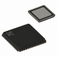
XE1205I074TRLF Semtech, XE1205I074TRLF Datasheet - Page 14

XE1205I074TRLF
Manufacturer Part Number
XE1205I074TRLF
Description
IC TXRX 433/868/915MHZ 48-VQFN
Manufacturer
Semtech
Datasheet
1.XE1205SKC915XE1.pdf
(48 pages)
Specifications of XE1205I074TRLF
Frequency
180MHz Center
Data Rate - Maximum
152.3kbps
Modulation Or Protocol
FSK
Applications
AMR, ISM, Home Automation, Process Control
Power - Output
0 ~ 15dBm
Sensitivity
-121dBm
Voltage - Supply
2.4 V ~ 3.6 V
Current - Receiving
14mA
Current - Transmitting
62mA
Data Interface
PCB, Surface Mount
Antenna Connector
PCB, Surface Mount
Operating Temperature
-40°C ~ 85°C
Package / Case
48-VQFN
Receiving Current
14mA
Transmitting Current
62mA
Data Rate
4.8Kbps
Modulation Type
FSK
Rf Ic Case Style
VQFN
No. Of Pins
48
Supply Voltage Range
2.4V To 3.6V
Operating Temperature (min)
-40C
Operating Temperature (max)
85C
Operating Temperature Classification
Industrial
Operating Supply Voltage (typ)
2.5/3.3V
Operating Supply Voltage (max)
3.6V
Rohs Compliant
Yes
Lead Free Status / RoHS Status
Lead free / RoHS Compliant
Memory Size
-
Lead Free Status / Rohs Status
Compliant
Other names
XE1205I074TR
5.2.3.6
XE1205 offers two possibilities to correct the RF frequency error either by using FEI block with external microcontroller
setting the corrected LO_Frequency or by using the internal Automatic Frequency error Cancellation (AFC).
When using FEI block,
without further calculation by a microcontroller since the PLL step is 500 Hz i.e.
number of step needed to compensate the frequency error .
Saout_fei is internally generated during a read sequence of register 12 in the same way as saout_rssi (refer to Figure 7).
To use AFC block, FEI block should be switched on by writing bit RXParam_FEI to ‘1’ then AFC should be started by
writing bit RX_Param:AFC_start to ‘1’. The LO_frequency error cancellation is effective providing bit RXParam_disable is
written to ‘0’ .Refer to previous chapter to guarantee proper behaviour of the FEI. RXParam_AFC_OK status register is
automatically set to ‘0’ when AFC is completed. RXParam_AFC_overflow will be automatically set to ‘1’ in case the
frequency error is too high to be automatically cancelled.
5.2.4
The DATA pin is bi-directional by default, and is used in both transmit and receive modes. In receive mode, DATA
represents demodulated received data. In transmit mode baseband data is applied to this pin.
Some applications may require a separate input and output for transmitted and received data respectively. In this case
the MCParam_Data_unidir configuration register bit must be set to ‘1’. The DATA pin is then set permanently to an
output for received data, and NSS_DATA is used as the input.
5.2.5
In this mode, the output of the bit synchronizer, i.e. the demodulated and resynchronized signal and the clock signal
DCLK are not sent directly to the output pins DATA and IRQ_1 (DCLK). These signals are used to store the
demodulated signal by packet of 8 bits in a 16 bytes FIFO. The following figure shows the receiver chain in this mode.
The FSK demodulator, bit synchronizer and pattern matching block work as described in section 5.2.2 but they are used
with two additional blocks, FIFO and SPI.
When the chip is in receive mode and the MCParam_Buffered_mode bit is set to high then all the blocks described
above are automatically enabled. In a normal communication frame the data stream comprises a 24 bit preamble,
pattern (refer to section 5.2.3.3) and the data. Upon receipt of a recognized pattern, the receiver recognizes the start of a
frame, strips off the preamble and pattern, then fills the FIFO with payload data to the microcontroller. This automated
data recovery reduces the overhead for the host controller.
The IRQParam_Start_fill bit determines how the FIFO is filled:
If IRQParam_Start_fill is low, data only fills the FIFO subject to a correct pattern match. Data is shifted into the pattern
recognition block which continuously compares the received data with the contents of the Reg_pattern(31:0)
configuration register. If a match occurs a start sequence is detected, and the internal output of the pattern matching
block is asserted for one bit length and the IRQParam_Start_detect bit is also asserted. This internal signal may be
mapped to the IRQ_0 output using interrupt signal mapping (please refer to section 5.2.2). Once a pattern match has
occurred, the pattern recognition block will remain inactive until IRQParam_Start_detect is re-asserted.
© Semtech 2008
DATA pin in bidirectional or unidirectional mode (continuous mode only)
Receiver in buffered mode
Frequency Error Correction
RXParam
_FEI_out(15:0) can directly be subtracted to the register MCParam_Freq_lo(15:0)
14
RXParam
_FEI_out (15:0) represents the
XE1205
www.semtech.com


