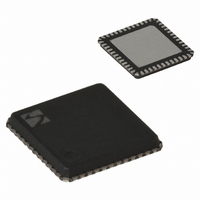
XE1205I074TRLF Semtech, XE1205I074TRLF Datasheet - Page 8

XE1205I074TRLF
Manufacturer Part Number
XE1205I074TRLF
Description
IC TXRX 433/868/915MHZ 48-VQFN
Manufacturer
Semtech
Datasheet
1.XE1205SKC915XE1.pdf
(48 pages)
Specifications of XE1205I074TRLF
Frequency
180MHz Center
Data Rate - Maximum
152.3kbps
Modulation Or Protocol
FSK
Applications
AMR, ISM, Home Automation, Process Control
Power - Output
0 ~ 15dBm
Sensitivity
-121dBm
Voltage - Supply
2.4 V ~ 3.6 V
Current - Receiving
14mA
Current - Transmitting
62mA
Data Interface
PCB, Surface Mount
Antenna Connector
PCB, Surface Mount
Operating Temperature
-40°C ~ 85°C
Package / Case
48-VQFN
Receiving Current
14mA
Transmitting Current
62mA
Data Rate
4.8Kbps
Modulation Type
FSK
Rf Ic Case Style
VQFN
No. Of Pins
48
Supply Voltage Range
2.4V To 3.6V
Operating Temperature (min)
-40C
Operating Temperature (max)
85C
Operating Temperature Classification
Industrial
Operating Supply Voltage (typ)
2.5/3.3V
Operating Supply Voltage (max)
3.6V
Rohs Compliant
Yes
Lead Free Status / RoHS Status
Lead free / RoHS Compliant
Memory Size
-
Lead Free Status / Rohs Status
Compliant
Other names
XE1205I074TR
The XE1205 is set to receive mode when MCParam_Select_mode is low by setting MCParam_Chip_mode(1:0) to “01”.
If MCParam_Select_mode is high the XE1205 is set to receive mode by setting SW(1:0) to “01”.
5.2.1
The LNA of the receiver has two programmable operation modes: the high sensitivity mode, Mode A, for reception of
weak signals; and the high linearity mode, Mode B, for strong signals. The operation mode is defined by the value of the
Rmode bit in RXParam_Rmode configuration register.
Mode A: High sensitivity mode, RFS approximately 13dB better than in Mode B (see 4.2.2, RFS parameter)
Mode B: High Linearity mode, IIP3 approximately 15dB higher than in Mode A (see 4.2.2, IIP3 parameter)
5.2.2
In receiver mode, two lines are dedicated to interrupt information. The interrupt pins are IRQ_0 and IRQ_1.
IRQ_0 has 3 selectable sources. IRQ_1 has 2 selectable sources. The two following tables summarize the interrupt
management.
5.2.3
In this mode, the receiver has two output signals indicating recovered clock DCLK and recovered NRZ bit DATA. DCLK
is connected to output pin IRQ_1 and DATA is connected to pin DATA configured in output mode. The bit synchronizer
controls the recovered clock signal, DCLK. If the bit synchronizer is enabled by setting the bit /RXParam_Disable_bitsync
to “0” (default value), the clock recovered from the incoming data stream appears at DCLK.
The function of the bit synchronizer is to remove glitches from the data stream and to provide a synchronous
clock at DCLK. The output DATA is valid at the rising edge of DCLK. The following diagram shows the receiver
chain operating in this mode
© Semtech 2008
5.2
IRQParam_RX_irq_0
IRQParam_RX_irq_1
RECEIVER SECTION
LNA & Receiver modes
Interrupt signal mapping
Receiver in continuous mode
00
01
10
11
00
01
10
11
00
01
10
11
00
01
10
11
MCParam_Buffered_mode
MCParam_Buffered_mode IRQ_1
Table 5: IRQ_0 interrupt sources in receive mode.
Table 6: IRQ_1 interrupt sources in receive mode.
0
0
0
0
1
1
1
1
0
0
0
0
1
1
1
1
8
IRQ_0
Output
Output
Output
Output
Output
Output
Output
Output
Output
Output
Output
Output
Output
Output
Output
Output
IRQ_0 Interrupt source
Pattern
RSSI_irq
Pattern
Pattern
No interrupt available
Write_byte
/fifoempty
Pattern
IRQ_1 Interrupt source
DCLK
DCLK
DCLK
DCLK
No interrupt available
Fifofull
RSSI_irq
RSSI_irq
XE1205
www.semtech.com


