CPV364M4KPBF Vishay, CPV364M4KPBF Datasheet - Page 8
CPV364M4KPBF
Manufacturer Part Number
CPV364M4KPBF
Description
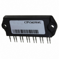
IGBT SIP MODULE 600V 13A IMS-2
Manufacturer
Vishay
Specifications of CPV364M4KPBF
Configuration
Three Phase Inverter
Voltage - Collector Emitter Breakdown (max)
600V
Vce(on) (max) @ Vge, Ic
1.8V @ 15V, 24A
Current - Collector (ic) (max)
24A
Current - Collector Cutoff (max)
250µA
Input Capacitance (cies) @ Vce
1.6nF @ 30V
Power - Max
63W
Input
Standard
Ntc Thermistor
No
Mounting Type
Through Hole
Package / Case
19-SIP (13 Leads), IMS-2
Collector- Emitter Voltage Vceo Max
600 V
Maximum Gate Emitter Voltage
+/- 20 V
Continuous Collector Current At 25 C
24 A
Maximum Operating Temperature
+ 150 C
Minimum Operating Temperature
- 55 C
Mounting Style
Through Hole
Dc Collector Current
24A
Collector Emitter Voltage Vces
600V
Power Dissipation Pd
63W
Collector Emitter Voltage V(br)ceo
600V
Operating Temperature Range
-55°C To +150°C
No. Of Pins
13
Lead Free Status / RoHS Status
Lead free / RoHS Compliant
Igbt Type
-
Lead Free Status / RoHS Status
Lead free / RoHS Compliant, Lead free / RoHS Compliant
Other names
*CPV364M4K
CPV364M4K
CPV364M4K
VS-CPV364M4K
VS-CPV364M4K
VS-CPV364M4KPBF
VS-CPV364M4KPBF
VSCPV364M4K
VSCPV364M4K
CPV364M4K
CPV364M4K
VS-CPV364M4K
VS-CPV364M4K
VS-CPV364M4KPBF
VS-CPV364M4KPBF
VSCPV364M4K
VSCPV364M4K
Available stocks
Company
Part Number
Manufacturer
Quantity
Price
Company:

Part Number:
CPV364M4KPBF
Manufacturer:
RENESAS
Quantity:
101


CPV364M4KPbF
Vishay High Power Products
Fig. 18a - Test Circuit for Measurement of I
www.vishay.com
8
Fig. 18b - Test Waveforms for Circuit of Fig. 18a,
of V
80 %
+Vge
CE
Ic
td(off)
10% Vce
Defining E
t1
I
rr
, t
430 µF
d(on)
Vce
90% Vge
, t
Ic
off
r
, t
tf
, t
d(off)
d(off)
t2
90% Ic
Same type
, t
device as
, t
For technical questions, contact: ind-modules@vishay.com
f
D.U.T.
LM
D.U.T.
Fig. 18e - Macro Waveforms for Figure 18a’s Test Circuit
f
Eoff =
, E
5% Ic
on
t0
, E
t1
Vce ic dt
t1+5µS
off(diode)
(Short Circuit Rated
IGBT SIP Module
, t
Ultrafast IGBT)
rr
t1
, Q
rr
t2
,
Vg GATE SIGNAL
DEVICE UNDER TEST
CURRENT D.U.T.
VOLTAGE IN D.U.T.
CURRENT IN D1
Fig. 18c - Test Waveforms for Circuit of Fig. 18a,
Fig. 18d - Test Waveforms for Circuit of Fig. 18a,
Vcc
Vpk
DIODE REVERSE
RECOVERY ENERGY
td(on)
Ic
10% +Vg
10% Ic
10% Vcc
tx
t1
Irr
Defining E
Vce
Defining E
tr
t3
5% Vce
trr
rec
90% Ic
on
, t
, t
GATE VOLTAGE D.U.T.
rr
+Vg
d(on)
, Q
DIODE RECOVERY
WAVEFORMS
t4
Document Number: 94488
Erec =
rr
, t
, I
10% Irr
r
rr
t2
Qrr =
Eon =
DUT VOLTAGE
AND CURRENT
Ipk
t3
Revision: 01-Sep-08
Vd id dt
t4
tx
t1
Vce ie dt
id dt
trr
t2
Ic
Vcc
Related parts for CPV364M4KPBF
Image
Part Number
Description
Manufacturer
Datasheet
Request
R

Part Number:
Description:
357-036-542-201 CARDEDGE 36POS DL .156 BLK LOPRO
Manufacturer:
Vishay
Datasheet:
Part Number:
Description:
357-036-542-201 CARDEDGE 36POS DL .156 BLK LOPRO
Manufacturer:
Vishay
Datasheet:
Part Number:
Description:
357-036-542-201 CARDEDGE 36POS DL .156 BLK LOPRO
Manufacturer:
Vishay
Datasheet:
Part Number:
Description:
357-036-542-201 CARDEDGE 36POS DL .156 BLK LOPRO
Manufacturer:
Vishay
Datasheet:
Part Number:
Description:
357-036-542-201 CARDEDGE 36POS DL .156 BLK LOPRO
Manufacturer:
Vishay
Datasheet:
Part Number:
Description:
357-036-542-201 CARDEDGE 36POS DL .156 BLK LOPRO
Manufacturer:
Vishay
Datasheet:
Part Number:
Description:
357-036-542-201 CARDEDGE 36POS DL .156 BLK LOPRO
Manufacturer:
Vishay
Datasheet:
Part Number:
Description:
357-036-542-201 CARDEDGE 36POS DL .156 BLK LOPRO
Manufacturer:
Vishay
Datasheet:
Part Number:
Description:
357-036-542-201 CARDEDGE 36POS DL .156 BLK LOPRO
Manufacturer:
Vishay
Datasheet:
Part Number:
Description:
357-036-542-201 CARDEDGE 36POS DL .156 BLK LOPRO
Manufacturer:
Vishay
Datasheet:
Part Number:
Description:
357-036-542-201 CARDEDGE 36POS DL .156 BLK LOPRO
Manufacturer:
Vishay
Datasheet:
Part Number:
Description:
357-036-542-201 CARDEDGE 36POS DL .156 BLK LOPRO
Manufacturer:
Vishay
Datasheet:
Part Number:
Description:
357-036-542-201 CARDEDGE 36POS DL .156 BLK LOPRO
Manufacturer:
Vishay
Datasheet:
Part Number:
Description:
357-036-542-201 CARDEDGE 36POS DL .156 BLK LOPRO
Manufacturer:
Vishay
Datasheet:
Part Number:
Description:
357-036-542-201 CARDEDGE 36POS DL .156 BLK LOPRO
Manufacturer:
Vishay
Datasheet: