PIC18LF24K22-I/SS Microchip Technology, PIC18LF24K22-I/SS Datasheet - Page 260
PIC18LF24K22-I/SS
Manufacturer Part Number
PIC18LF24K22-I/SS
Description
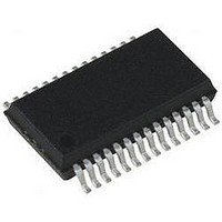
IC PIC MCU 16KB FLASH 28SSOP
Manufacturer
Microchip Technology
Series
PIC® XLP™ 18Fr
Specifications of PIC18LF24K22-I/SS
Core Size
8-Bit
Program Memory Size
16KB (8K x 16)
Core Processor
PIC
Speed
64MHz
Connectivity
I²C, SPI, UART/USART
Peripherals
Brown-out Detect/Reset, HLVD, POR, PWM, WDT
Number Of I /o
24
Program Memory Type
FLASH
Eeprom Size
256 x 8
Ram Size
768 x 8
Voltage - Supply (vcc/vdd)
1.8 V ~ 3.6 V
Data Converters
A/D 19x10b
Oscillator Type
Internal
Operating Temperature
-40°C ~ 85°C
Package / Case
28-SSOP (0.200", 5.30mm Width)
Controller Family/series
PIC18
No. Of I/o's
25
Eeprom Memory Size
256Byte
Ram Memory Size
768Byte
Cpu Speed
64MHz
No. Of Timers
7
Lead Free Status / RoHS Status
Lead free / RoHS Compliant


PIC18(L)F2X/4XK22
REGISTER 15-4:
REGISTER 15-5:
DS41412D-page 260
bit 0
Note 1:
bit 7
Legend:
R = Readable bit
u = Bit is unchanged
‘1’ = Bit is set
bit 7-1
bit 0
R/W-1
MSK7
2:
3:
For daisy-chained SPI operation; allows the user to ignore all but the last received byte. SSPxOV is still
set when a new byte is received and BF = 1, but hardware continues to write the most recent byte to
SSPxBUF.
This bit has no effect in Slave modes for which Start and Stop condition detection is explicitly listed as
enabled.
The ACKTIM Status bit is active only when the AHEN bit or DHEN bit is set.
DHEN: Data Hold Enable bit (I
1 = Following the 8th falling edge of SCLx for a received data byte; slave hardware clears the CKP bit
0 = Data holding is disabled
MSK<7:1>: Mask bits
1 = The received address bit n is compared to SSPxADD<n> to detect I
0 = The received address bit n is not used to detect I
MSK<0>: Mask bit for I
I
1 = The received address bit 0 is compared to SSPxADD<0> to detect I
0 = The received address bit 0 is not used to detect I
I
2
2
C Slave mode, 10-bit address (SSPxM<3:0> = 0111 or 1111):
C Slave mode, 7-bit address, the bit is ignored
R/W-1
MSK6
of the SSPxCON1 register and SCLx is held low.
SSPxCON3: SSPx CONTROL REGISTER 3 (CONTINUED)
SSPxMSK: SSPx MASK REGISTER
W = Writable bit
x = Bit is unknown
‘0’ = Bit is cleared
R/W-1
MSK5
2
C Slave mode, 10-bit Address
2
C Slave mode only)
R/W-1
MSK4
Preliminary
U = Unimplemented bit, read as ‘0’
-n/n = Value at POR and BOR/Value at all other Resets
R/W-1
MSK3
2
2
C address match
C address match
R/W-1
MSK2
2010 Microchip Technology Inc.
2
2
C address match
C address match
R/W-1
MSK1
R/W-1
MSK0
bit 0
Related parts for PIC18LF24K22-I/SS
Image
Part Number
Description
Manufacturer
Datasheet
Request
R

Part Number:
Description:
Manufacturer:
Microchip Technology Inc.
Datasheet:
Part Number:
Description:
Manufacturer:
Microchip Technology Inc.
Datasheet:
Part Number:
Description:
Manufacturer:
Microchip Technology Inc.
Datasheet:
Part Number:
Description:
Manufacturer:
Microchip Technology Inc.
Datasheet:
Part Number:
Description:
Manufacturer:
Microchip Technology Inc.
Datasheet:
Part Number:
Description:
Manufacturer:
Microchip Technology Inc.
Datasheet:
Part Number:
Description:
Manufacturer:
Microchip Technology Inc.
Datasheet:
Part Number:
Description:
Manufacturer:
Microchip Technology Inc.
Datasheet: