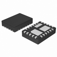
NUS6160MNTWG ON Semiconductor, NUS6160MNTWG Datasheet - Page 12

NUS6160MNTWG
Manufacturer Part Number
NUS6160MNTWG
Description
IC OVP LOW PRO W/MOSFET 22-QFN
Manufacturer
ON Semiconductor
Datasheet
1.NUS6160MNTWG.pdf
(13 pages)
Specifications of NUS6160MNTWG
Voltage - Working
1.2 ~ 20V
Technology
Mixed Technology
Number Of Circuits
1
Applications
General Purpose
Package / Case
22-TQFN Exposed Pad
Lead Free Status / RoHS Status
Lead free / RoHS Compliant
Power (watts)
-
Voltage - Clamping
-
Operational Description
positive voltages up to 20 V. A P−Channel FET protects the
load connected on the V
conditions. The Output follows the V
threshold is reached.
Undervoltage Lockout (UVLO)
device has a built−in undervoltage lock out (UVLO) circuit.
As the input ramps from 0 V, the output remains
disconnected from input until the V
nominal. The FLAG output is pulled to low as long as V
does not reach the UVLO threshold. This circuit
incorporates hysteresis on the UVLO pin to provide noise
immunity to transient condition.
Overvoltage Lockout (OVLO)
overvoltage, the device has a built−in overvoltage lock out
(OVLO) circuit. During an overvoltage condition, the
output remains disabled until the input voltage is reduced to
below the OVLO hysteresis level. The FLAG output is tied
to low until V
incorporates hysteresis on the OVLO pin to provide noise
immunity from transient conditions.
FLAG Output
external systems that a fault has occurred. This pin goes low
as soon as the OVLO threshold is exceeded. When V
recovers to its normal range the FLAG is set high.
resistor (typically 1 MW − Minimum 10 kW) must be
provided to V
EN Input
low or connected to ground. A high level on the pin
disconnects the OUT Pin from IN Pin. EN does not override
an OVLO or UVLO fault.
Internal PMOS FET
connects the input to the output pin. This FET is turned off
The NUS6160 provides overvoltage protection for
To ensure proper operation under all conditions, the
To protect connected systems on V
The NUS6160 provides a FLAG output, which alerts
The FLAG Pin is an open drain output, thus a pullup
To enable normal operation, the EN pin shall be forced
The NUS6160 includes an internal PMOS FET which
Figure 28. Output Characteristic vs. V
battery
in
.
is higher than OVLO. This circuit
out
pin, against positive overvoltage
in
BUS
voltage is above 3.2 V
level until OVLO
out
in
Pin from
in
http://onsemi.com
level
in
12
in the event of an overvoltage condition to protect the output
from a positive overvoltage condition. The low R
during normal operation will minimize the voltage drop
across the device. (See Figure 16).
ESD Tests
IEC61000*4*2, level 4 (Input pin, 1 mF mounted on
board). For the air discharge condition, V
to $15 kV. In the contact condition, V
±8 kV ESD. Please refer to Figure 29 to see the IEC
61000−4−2 electrostatic discharge waveform.
Thermal Impedance
equivalent thetas are given for this device rather than the
individual thetas. To calculate the junction temperatures of
a single die, the total power must be used. For example,
given the following parameters, the die temperatures will be
as shown:
I
R
R
FET
Board copper area = 161 mm
Calculate the individual power dissipations:
P
P
P
P
From the Maximum ratings table for thetas, 161 mm
1 V drop across FET
OVP FET
FET
FET
The die temperature rises above ambient are:
T
T
T
dc
OVP
SW
REG
TOT
OVP
SW
REG
DS(on)
DS(on)
The NUS6160 meets the requirements of
Due to cross heating of the three dice in the package, the
= 500 mA
reg
SW
REG
= (0.50 A)
= 49°C/W x 0.594 W = 29°C
= 0.076 + 0.018 + 0.50 = 0.594 W
= (0.50 A)
= 0.50 A x 1.0 V = 0.50 W
= 53°C/W x 0.594 W = 32°C
= 92°C/W x 0.594 W = 55°C
has a 1.0 V Drop
OVP = 305 mW
FETsw = 72 mW
Figure 29. IEC 61000−4−2 Curve
2
2
x .072 W = 0.018 W
x .305 W = 0.076 W
53°C/W
49°C/W
92°C/W
REG
:
2
in
is protected up to
in
is protected up
ds(on)
2
and
the
,


