BLF573,112 NXP Semiconductors, BLF573,112 Datasheet
BLF573,112
Specifications of BLF573,112
Available stocks


Related parts for BLF573,112


BLF573,112 Summary of contents
Page 1
BLF573; BLF573S HF / VHF power LDMOS transistor Rev. 3 — 8 July 2010 1. Product profile 1.1 General description A 300 W LDMOS RF power transistor for broadcast applications and industrial, scientific and medical applications in the HF to ...
Page 2
... NXP Semiconductors 2. Pinning information Table 2. Pin BLF573 (SOT502A BLF573S (SOT502B [1] Connected to flange. 3. Ordering information Table 3. Type number Package BLF573 BLF573S 4. Limiting values Table 4. In accordance with the Absolute Maximum Rating System (IEC 60134). Symbol stg Thermal characteristics Table 5. Symbol R th(j-c) [1] R th(j-c) ...
Page 3
... NXP Semiconductors 6. Characteristics Table 6. ° Symbol Parameter V (BR)DSS V GS(th) V GSq I DSS I DSX I GSS DS(on iss C oss Table 7. Mode of operation: CW 225 MHz; RF performance at V unless otherwise specified class-AB production test circuit. Symbol Parameter η D BLF573_BLF573S Product data sheet DC characteristics C unless otherwise specified. ...
Page 4
... NXP Semiconductors Fig 1. 6.1 Ruggedness in class-AB operation The BLF573 and BLF573S are capable of withstanding a load mismatch corresponding to VSWR = through all phases under the following conditions 900 mA Application information 7.1 Impedance information Table 8. Measured Z f MHz 225 Fig 2. BLF573_BLF573S Product data sheet ...
Page 5
... NXP Semiconductors 7.2 Reliability Years (1) T (2) T (3) T (4) T (5) T (6) T (7) T (8) T (9) T (10) T (11) T Fig 3. BLF573_BLF573S Product data sheet TTF (0.1 % failure fraction). = 100 ° 110 ° 120 ° 130 ° 140 ° 150 ° 160 ° 170 ° 180 ° ...
Page 6
... NXP Semiconductors 8. Test information 8.1 RF Performance The following figures are measured in a class-AB production test circuit. 8.1.1 1-Tone (dB η 100 200 900 mA 225 MHz Fig 4. Power gain and drain efficiency as functions of load power; typical values BLF573_BLF573S Product data sheet 001aaj612 80 30 η ...
Page 7
... NXP Semiconductors 900 mA 225 MHz ( 55.2 dBm (330 W) L(1dB) ( 55.8 dBm (380 W) L(3dB) Fig 6. Load power as function of input power; typical values BLF573_BLF573S Product data sheet (dBm) Ideal ( All information provided in this document is subject to legal disclaimers. Rev. 3 — 8 July 2010 BLF573; BLF573S ...
Page 8
... NXP Semiconductors 8.1.2 2-Tone (dB η 100 200 900 mA 225.05 MHz. 2 Fig 7. Power gain and drain efficiency as functions of peak envelope load power; typical values 8.2 Test circuit Table 9. List of components For production test circuit, see Figure 9 Printed-Circuit Board (PCB): Rogers 5880; μ ...
Page 9
... NXP Semiconductors Table 9. List of components For production test circuit, see Figure 9 Printed-Circuit Board (PCB): Rogers 5880; μ thickness copper plating = 35 m. Component Description C15 multilayer ceramic chip capacitor C16 multilayer ceramic chip capacitor C17 multilayer ceramic chip capacitor C19 electrolytic capacitor ...
Page 10
... NXP Semiconductors C1 C2 Fig 10. Component layout for class-AB production test circuit BLF573_BLF573S Product data sheet B1 C9 C20 C10 All information provided in this document is subject to legal disclaimers. Rev. 3 — 8 July 2010 BLF573; BLF573S HF / VHF power LDMOS transistor C19 C13 C14 L2 C17 C11 C12 ...
Page 11
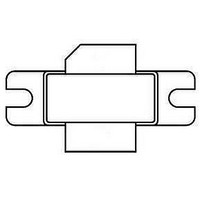
... NXP Semiconductors 9. Package outline Flanged LDMOST ceramic package; 2 mounting holes; 2 leads DIMENSIONS (millimetre dimensions are derived from the original inch dimensions) c UNIT 12.83 4.72 0.15 20.02 mm 12.57 3.43 0.08 19.61 0.505 0.186 0.006 0.788 inches 0.135 0.495 0.772 0.003 OUTLINE VERSION ...
Page 12
... NXP Semiconductors Earless flanged LDMOST ceramic package; 2 leads DIMENSIONS (millimetre dimensions are derived from the original inch dimensions) c UNIT 12.83 4.72 0.15 20.02 mm 12.57 3.43 0.08 19.61 0.505 0.186 0.006 0.788 inches 0.135 0.495 0.772 0.003 OUTLINE VERSION IEC SOT502B Fig 12. Package outline SOT502B ...
Page 13
... NXP Semiconductors 10. Abbreviations Table 10. Acronym CW EDGE GSM HF LDMOS LDMOST RF SMD TTF VHF VSWR 11. Revision history Table 11. Revision history Document ID Release date BLF573_BLF573S v.3 20100708 Modifications: BLF573S v.2 20090217 BLF573S v.1 20081208 BLF573_BLF573S Product data sheet Abbreviations Description Continuous Wave Enhanced Data rates for GSM Evolution ...
Page 14
... In no event shall NXP Semiconductors be liable for any indirect, incidental, punitive, special or consequential damages (including - without limitation - lost profits, lost savings, business interruption, costs related to the removal or ...
Page 15
... Product data sheet NXP Semiconductors’ specifications such use shall be solely at customer’s own risk, and (c) customer fully indemnifies NXP Semiconductors for any liability, damages or failed product claims resulting from customer design and use of the product for automotive applications beyond NXP Semiconductors’ ...
Page 16
... NXP Semiconductors 14. Contents 1 Product profile . . . . . . . . . . . . . . . . . . . . . . . . . . 1 1.1 General description . . . . . . . . . . . . . . . . . . . . . 1 1.2 Features and benefits . . . . . . . . . . . . . . . . . . . . 1 1.3 Applications . . . . . . . . . . . . . . . . . . . . . . . . . . . 1 2 Pinning information . . . . . . . . . . . . . . . . . . . . . . 2 3 Ordering information . . . . . . . . . . . . . . . . . . . . . 2 4 Limiting values Thermal characteristics . . . . . . . . . . . . . . . . . . 2 6 Characteristics . . . . . . . . . . . . . . . . . . . . . . . . . . 3 6.1 Ruggedness in class-AB operation . . . . . . . . . 4 7 Application information 7.1 Impedance information . . . . . . . . . . . . . . . . . . . 4 7.2 Reliability . . . . . . . . . . . . . . . . . . . . . . . . . . . . . 5 8 Test information . . . . . . . . . . . . . . . . . . . . . . . . . 6 8 ...