M052LAN Nuvoton Technology Corporation of America, M052LAN Datasheet
M052LAN
Specifications of M052LAN
Available stocks


Related parts for M052LAN

M052LAN Summary of contents
Page 1
NuMicro M051 Series Technical Reference Manual 32-BIT MICROCONTROLLER NuMicro M051 Technical Reference Manual - 1 - ™ ARM Cortex ™ Series Publication Release Date: Sep 14, 2010 Revision V1.2 -M0 ...
Page 2
NuMicro M051 TABLE OF CONTENTS 1 GENERAL DESCRIPTION ∙∙∙∙∙∙∙∙∙∙∙∙∙∙∙∙∙∙∙∙∙∙∙∙∙∙∙∙∙∙∙∙∙∙∙∙∙∙∙∙∙∙∙∙∙∙∙∙∙∙∙∙∙∙∙∙∙∙∙∙∙∙∙∙∙∙∙∙∙∙∙∙∙∙∙∙∙∙∙∙∙∙∙∙∙∙∙∙∙∙∙∙∙∙∙∙∙∙∙∙∙∙∙∙∙∙∙∙∙∙∙11 2 FEATURES∙∙∙∙∙∙∙∙∙∙∙∙∙∙∙∙∙∙∙∙∙∙∙∙∙∙∙∙∙∙∙∙∙∙∙∙∙∙∙∙∙∙∙∙∙∙∙∙∙∙∙∙∙∙∙∙∙∙∙∙∙∙∙∙∙∙∙∙∙∙∙∙∙∙∙∙∙∙∙∙∙∙∙∙∙∙∙∙∙∙∙∙∙∙∙∙∙∙∙∙∙∙∙∙∙∙∙∙∙∙∙∙∙∙∙∙∙∙∙∙∙∙∙∙∙∙∙∙∙∙∙∙∙∙∙∙12 3 BLOCK DIAGRAM∙∙∙∙∙∙∙∙∙∙∙∙∙∙∙∙∙∙∙∙∙∙∙∙∙∙∙∙∙∙∙∙∙∙∙∙∙∙∙∙∙∙∙∙∙∙∙∙∙∙∙∙∙∙∙∙∙∙∙∙∙∙∙∙∙∙∙∙∙∙∙∙∙∙∙∙∙∙∙∙∙∙∙∙∙∙∙∙∙∙∙∙∙∙∙∙∙∙∙∙∙∙∙∙∙∙∙∙∙∙∙∙∙∙∙∙∙∙∙∙∙∙∙∙17 SELECTION TABLE ∙∙∙∙∙∙∙∙∙∙∙∙∙∙∙∙∙∙∙∙∙∙∙∙∙∙∙∙∙∙∙∙∙∙∙∙∙∙∙∙∙∙∙∙∙∙∙∙∙∙∙∙∙∙∙∙∙∙∙∙∙∙∙∙∙∙∙∙∙∙∙∙∙∙∙∙∙∙∙∙∙∙∙∙∙∙∙∙∙∙∙∙∙∙∙∙∙∙∙∙∙∙∙∙∙∙∙∙∙∙∙∙∙∙∙∙∙∙∙∙∙18 4 PIN CONFIGURATION ∙∙∙∙∙∙∙∙∙∙∙∙∙∙∙∙∙∙∙∙∙∙∙∙∙∙∙∙∙∙∙∙∙∙∙∙∙∙∙∙∙∙∙∙∙∙∙∙∙∙∙∙∙∙∙∙∙∙∙∙∙∙∙∙∙∙∙∙∙∙∙∙∙∙∙∙∙∙∙∙∙∙∙∙∙∙∙∙∙∙∙∙∙∙∙∙∙∙∙∙∙∙∙∙∙∙∙∙∙∙∙∙∙∙∙∙∙20 5 5.1 QFN 33 pin ∙∙∙∙∙∙∙∙∙∙∙∙∙∙∙∙∙∙∙∙∙∙∙∙∙∙∙∙∙∙∙∙∙∙∙∙∙∙∙∙∙∙∙∙∙∙∙∙∙∙∙∙∙∙∙∙∙∙∙∙∙∙∙∙∙∙∙∙∙∙∙∙∙∙∙∙∙∙∙∙∙∙∙∙∙∙∙∙∙∙∙∙∙∙∙∙∙∙∙∙∙∙∙∙∙∙∙∙∙∙∙∙∙∙∙∙∙∙∙∙∙∙∙∙∙∙∙∙∙∙∙∙∙∙∙∙∙∙∙∙∙∙∙∙21 5.2 LQFP 48 pin ∙∙∙∙∙∙∙∙∙∙∙∙∙∙∙∙∙∙∙∙∙∙∙∙∙∙∙∙∙∙∙∙∙∙∙∙∙∙∙∙∙∙∙∙∙∙∙∙∙∙∙∙∙∙∙∙∙∙∙∙∙∙∙∙∙∙∙∙∙∙∙∙∙∙∙∙∙∙∙∙∙∙∙∙∙∙∙∙∙∙∙∙∙∙∙∙∙∙∙∙∙∙∙∙∙∙∙∙∙∙∙∙∙∙∙∙∙∙∙∙∙∙∙∙∙∙∙∙∙∙∙∙∙∙∙∙∙∙∙∙∙∙22 5.3 Pin Description∙∙∙∙∙∙∙∙∙∙∙∙∙∙∙∙∙∙∙∙∙∙∙∙∙∙∙∙∙∙∙∙∙∙∙∙∙∙∙∙∙∙∙∙∙∙∙∙∙∙∙∙∙∙∙∙∙∙∙∙∙∙∙∙∙∙∙∙∙∙∙∙∙∙∙∙∙∙∙∙∙∙∙∙∙∙∙∙∙∙∙∙∙∙∙∙∙∙∙∙∙∙∙∙∙∙∙∙∙∙∙∙∙∙∙∙∙∙∙∙∙∙∙∙∙∙∙∙∙∙∙∙∙∙∙∙∙∙23 6 FUNCTIONAL DESCRIPTION ∙∙∙∙∙∙∙∙∙∙∙∙∙∙∙∙∙∙∙∙∙∙∙∙∙∙∙∙∙∙∙∙∙∙∙∙∙∙∙∙∙∙∙∙∙∙∙∙∙∙∙∙∙∙∙∙∙∙∙∙∙∙∙∙∙∙∙∙∙∙∙∙∙∙∙∙∙∙∙∙∙∙∙∙∙∙∙∙∙∙∙∙∙∙∙∙∙∙∙∙∙∙∙∙∙26 6.1 ...
Page 3
NuMicro M051 Series Technical Reference Manual 6.5.3 Function Description ∙∙∙∙∙∙∙∙∙∙∙∙∙∙∙∙∙∙∙∙∙∙∙∙∙∙∙∙∙∙∙∙∙∙∙∙∙∙∙∙∙∙∙∙∙∙∙∙∙∙∙∙∙∙∙∙∙∙∙∙∙∙∙∙∙∙∙∙∙∙∙∙∙∙∙∙∙∙∙∙∙∙∙∙∙∙∙∙∙∙∙∙∙∙∙∙∙∙∙∙∙∙∙∙∙∙∙∙∙∙∙∙∙160 6.5.4 I2C Protocol Registers∙∙∙∙∙∙∙∙∙∙∙∙∙∙∙∙∙∙∙∙∙∙∙∙∙∙∙∙∙∙∙∙∙∙∙∙∙∙∙∙∙∙∙∙∙∙∙∙∙∙∙∙∙∙∙∙∙∙∙∙∙∙∙∙∙∙∙∙∙∙∙∙∙∙∙∙∙∙∙∙∙∙∙∙∙∙∙∙∙∙∙∙∙∙∙∙∙∙∙∙∙∙∙∙∙∙∙∙∙∙164 6.5.5 I2C Controller Registers Map ∙∙∙∙∙∙∙∙∙∙∙∙∙∙∙∙∙∙∙∙∙∙∙∙∙∙∙∙∙∙∙∙∙∙∙∙∙∙∙∙∙∙∙∙∙∙∙∙∙∙∙∙∙∙∙∙∙∙∙∙∙∙∙∙∙∙∙∙∙∙∙∙∙∙∙∙∙∙∙∙∙∙∙∙∙∙∙∙∙∙∙∙∙∙∙∙∙∙168 6.5.6 I2C Controller Registers Description∙∙∙∙∙∙∙∙∙∙∙∙∙∙∙∙∙∙∙∙∙∙∙∙∙∙∙∙∙∙∙∙∙∙∙∙∙∙∙∙∙∙∙∙∙∙∙∙∙∙∙∙∙∙∙∙∙∙∙∙∙∙∙∙∙∙∙∙∙∙∙∙∙∙∙∙∙∙∙∙∙∙∙∙∙∙169 6.5.7 Modes of Operation ∙∙∙∙∙∙∙∙∙∙∙∙∙∙∙∙∙∙∙∙∙∙∙∙∙∙∙∙∙∙∙∙∙∙∙∙∙∙∙∙∙∙∙∙∙∙∙∙∙∙∙∙∙∙∙∙∙∙∙∙∙∙∙∙∙∙∙∙∙∙∙∙∙∙∙∙∙∙∙∙∙∙∙∙∙∙∙∙∙∙∙∙∙∙∙∙∙∙∙∙∙∙∙∙∙∙∙∙∙∙∙∙∙∙177 6.5.8 Data Transfer Flow in Five Operating Modes ∙∙∙∙∙∙∙∙∙∙∙∙∙∙∙∙∙∙∙∙∙∙∙∙∙∙∙∙∙∙∙∙∙∙∙∙∙∙∙∙∙∙∙∙∙∙∙∙∙∙∙∙∙∙∙∙∙∙∙∙∙∙∙∙∙∙∙∙∙∙∙178 ...
Page 4
NuMicro M051 6.11.2 Features∙∙∙∙∙∙∙∙∙∙∙∙∙∙∙∙∙∙∙∙∙∙∙∙∙∙∙∙∙∙∙∙∙∙∙∙∙∙∙∙∙∙∙∙∙∙∙∙∙∙∙∙∙∙∙∙∙∙∙∙∙∙∙∙∙∙∙∙∙∙∙∙∙∙∙∙∙∙∙∙∙∙∙∙∙∙∙∙∙∙∙∙∙∙∙∙∙∙∙∙∙∙∙∙∙∙∙∙∙∙∙∙∙∙∙∙∙∙∙∙∙∙∙∙∙∙∙∙∙∙∙∙∙∙309 6.11.3 ADC Block Diagram∙∙∙∙∙∙∙∙∙∙∙∙∙∙∙∙∙∙∙∙∙∙∙∙∙∙∙∙∙∙∙∙∙∙∙∙∙∙∙∙∙∙∙∙∙∙∙∙∙∙∙∙∙∙∙∙∙∙∙∙∙∙∙∙∙∙∙∙∙∙∙∙∙∙∙∙∙∙∙∙∙∙∙∙∙∙∙∙∙∙∙∙∙∙∙∙∙∙∙∙∙∙∙∙∙∙∙∙∙∙∙∙∙∙311 6.11.4 ADC Operation Procedure∙∙∙∙∙∙∙∙∙∙∙∙∙∙∙∙∙∙∙∙∙∙∙∙∙∙∙∙∙∙∙∙∙∙∙∙∙∙∙∙∙∙∙∙∙∙∙∙∙∙∙∙∙∙∙∙∙∙∙∙∙∙∙∙∙∙∙∙∙∙∙∙∙∙∙∙∙∙∙∙∙∙∙∙∙∙∙∙∙∙∙∙∙∙∙∙∙∙∙∙∙∙∙313 6.11.5 ADC Controller Registers Map∙∙∙∙∙∙∙∙∙∙∙∙∙∙∙∙∙∙∙∙∙∙∙∙∙∙∙∙∙∙∙∙∙∙∙∙∙∙∙∙∙∙∙∙∙∙∙∙∙∙∙∙∙∙∙∙∙∙∙∙∙∙∙∙∙∙∙∙∙∙∙∙∙∙∙∙∙∙∙∙∙∙∙∙∙∙∙∙∙∙∙∙∙∙∙∙320 6.11.6 ADC Controller Registers Description∙∙∙∙∙∙∙∙∙∙∙∙∙∙∙∙∙∙∙∙∙∙∙∙∙∙∙∙∙∙∙∙∙∙∙∙∙∙∙∙∙∙∙∙∙∙∙∙∙∙∙∙∙∙∙∙∙∙∙∙∙∙∙∙∙∙∙∙∙∙∙∙∙∙∙∙∙∙∙∙∙∙∙∙321 6.12 External Bus Interface (EBI) ∙∙∙∙∙∙∙∙∙∙∙∙∙∙∙∙∙∙∙∙∙∙∙∙∙∙∙∙∙∙∙∙∙∙∙∙∙∙∙∙∙∙∙∙∙∙∙∙∙∙∙∙∙∙∙∙∙∙∙∙∙∙∙∙∙∙∙∙∙∙∙∙∙∙∙∙∙∙∙∙∙∙∙∙∙∙∙∙∙∙∙∙∙∙∙∙∙∙∙∙∙∙∙∙∙∙∙∙∙∙∙333 6.12.1 Overview∙∙∙∙∙∙∙∙∙∙∙∙∙∙∙∙∙∙∙∙∙∙∙∙∙∙∙∙∙∙∙∙∙∙∙∙∙∙∙∙∙∙∙∙∙∙∙∙∙∙∙∙∙∙∙∙∙∙∙∙∙∙∙∙∙∙∙∙∙∙∙∙∙∙∙∙∙∙∙∙∙∙∙∙∙∙∙∙∙∙∙∙∙∙∙∙∙∙∙∙∙∙∙∙∙∙∙∙∙∙∙∙∙∙∙∙∙∙∙∙∙∙∙∙∙∙∙∙∙∙∙∙∙333 6.12.2 Features∙∙∙∙∙∙∙∙∙∙∙∙∙∙∙∙∙∙∙∙∙∙∙∙∙∙∙∙∙∙∙∙∙∙∙∙∙∙∙∙∙∙∙∙∙∙∙∙∙∙∙∙∙∙∙∙∙∙∙∙∙∙∙∙∙∙∙∙∙∙∙∙∙∙∙∙∙∙∙∙∙∙∙∙∙∙∙∙∙∙∙∙∙∙∙∙∙∙∙∙∙∙∙∙∙∙∙∙∙∙∙∙∙∙∙∙∙∙∙∙∙∙∙∙∙∙∙∙∙∙∙∙∙∙333 6.12.3 EBI Block Diagram∙∙∙∙∙∙∙∙∙∙∙∙∙∙∙∙∙∙∙∙∙∙∙∙∙∙∙∙∙∙∙∙∙∙∙∙∙∙∙∙∙∙∙∙∙∙∙∙∙∙∙∙∙∙∙∙∙∙∙∙∙∙∙∙∙∙∙∙∙∙∙∙∙∙∙∙∙∙∙∙∙∙∙∙∙∙∙∙∙∙∙∙∙∙∙∙∙∙∙∙∙∙∙∙∙∙∙∙∙∙∙∙∙∙∙∙334 6.12.4 Operation Procedure ∙∙∙∙∙∙∙∙∙∙∙∙∙∙∙∙∙∙∙∙∙∙∙∙∙∙∙∙∙∙∙∙∙∙∙∙∙∙∙∙∙∙∙∙∙∙∙∙∙∙∙∙∙∙∙∙∙∙∙∙∙∙∙∙∙∙∙∙∙∙∙∙∙∙∙∙∙∙∙∙∙∙∙∙∙∙∙∙∙∙∙∙∙∙∙∙∙∙∙∙∙∙∙∙∙∙∙∙∙∙∙∙335 ...
Page 5
NuMicro M051 Series Technical Reference Manual 10 PACKAGE DIMENSIONS∙∙∙∙∙∙∙∙∙∙∙∙∙∙∙∙∙∙∙∙∙∙∙∙∙∙∙∙∙∙∙∙∙∙∙∙∙∙∙∙∙∙∙∙∙∙∙∙∙∙∙∙∙∙∙∙∙∙∙∙∙∙∙∙∙∙∙∙∙∙∙∙∙∙∙∙∙∙∙∙∙∙∙∙∙∙∙∙∙∙∙∙∙∙∙∙∙∙∙∙∙∙∙∙∙∙∙∙∙∙∙ 381 2 10.1 LQFP-48 (7x7x1.4mm Footprint 2.0mm) ∙∙∙∙∙∙∙∙∙∙∙∙∙∙∙∙∙∙∙∙∙∙∙∙∙∙∙∙∙∙∙∙∙∙∙∙∙∙∙∙∙∙∙∙∙∙∙∙∙∙∙∙∙∙∙∙∙∙∙∙∙∙∙∙∙∙∙∙∙∙∙∙∙∙∙∙∙∙∙∙∙∙∙∙∙∙∙∙381 2 10.2 QFN-33 (5X5 mm , Thickness 0.8mm, Pitch 0.5 mm)∙∙∙∙∙∙∙∙∙∙∙∙∙∙∙∙∙∙∙∙∙∙∙∙∙∙∙∙∙∙∙∙∙∙∙∙∙∙∙∙∙∙∙∙∙∙∙∙∙∙∙∙∙∙∙∙∙∙∙∙∙∙∙∙∙∙∙∙382 11 REVISION HISTORY∙∙∙∙∙∙∙∙∙∙∙∙∙∙∙∙∙∙∙∙∙∙∙∙∙∙∙∙∙∙∙∙∙∙∙∙∙∙∙∙∙∙∙∙∙∙∙∙∙∙∙∙∙∙∙∙∙∙∙∙∙∙∙∙∙∙∙∙∙∙∙∙∙∙∙∙∙∙∙∙∙∙∙∙∙∙∙∙∙∙∙∙∙∙∙∙∙∙∙∙∙∙∙∙∙∙∙∙∙∙∙∙∙∙∙∙∙∙∙ 383 Publication Release Date: Sept 14, 2010 - ...
Page 6
NuMicro M051 LIST OF FIGURES Figure 5.1-1 NuMicro™ M051 Series Block Diagram..................................................................... 17 Figure 5.1-1 NuMicro™ Naming Rule............................................................................................. 19 Figure 5.1-1 NuMicro™ M051 Series QFN33 Pin Diagram............................................................ 21 Figure 5.2-1 NuMicro™ M051 Series LQFP-48 Pin Diagram........................................................ 22 Figure 6.1-1 Functional ...
Page 7
NuMicro M051 Series Technical Reference Manual Figure 6.5-15 GC Mode ............................................................................................................... 185 Figure 6.6-1 PWM Generator 0 Clock Source Control................................................................. 188 Figure 6.6-2 PWM Generator 0 Architecture Diagram................................................................. 189 Figure 6.6-3 PWM Generator 2 Clock Source Control................................................................. 190 Figure ...
Page 8
NuMicro M051 Figure 6.9-3 Watchdog Timer Block Diagram.............................................................................. 267 Figure 6.10-1 UART Clock Control Diagram................................................................................ 275 Figure 6.10-2 UART Block Diagram............................................................................................. 276 Figure 6.10-3 Auto Flow Control Block Diagram.......................................................................... 278 Figure 6.10-4 IrDA Block Diagram ............................................................................................... 279 Figure 6.10-5 ...
Page 9
NuMicro M051 Series Technical Reference Manual Figure 9.3-1 Typical Crystal Application Circuit ........................................................................... 374 Figure 9.5-1 SPI Master timing .................................................................................................... 380 Figure 9.5-2 SPI Slave timing ...................................................................................................... 380 Publication Release Date: Sept 14, 2010 - 9 - Revision V1.2 ...
Page 10
NuMicro M051 LIST OF TABLES Table 5.1-1 NuMicro™ M051 Series Product Selection Guide ...................................................... 18 Table 5.3-1 NuMicro™ M051 Series Pin Description ..................................................................... 25 Table 6.2-1 Address Space Assignments for On-Chip Modules ................................................... 31 Table 6.2-2 Exception Model ......................................................................................................... 72 ...
Page 11
NuMicro M051 Series Technical Reference Manual 1 GENERAL DESCRIPTION ™ The NuMicro M051 series is a 32-bit microcontroller with embedded ARM industrial control and applications which need rich communication interfaces. The Cortex the newest ARM embedded processor with 32-bit ...
Page 12
NuMicro M051 2 FEATURES Core ® ™ ARM Cortex -M0 core runs MHz. One 24-bit system timer. Supports low power sleep-mode. A single-cycle 32-bit hardware multiplier. NVIC for the 32 interrupt inputs, each with 4-levels of priority. ...
Page 13
NuMicro M051 Series Technical Reference Manual Four I/O modes: Quasi bi-direction Push-Pull output Open-Drain output Input only with high impendence TTL/Schmitt trigger input selectable I/O pin can be configured as interrupt source with edge/level setting Supports high driver and ...
Page 14
NuMicro M051 Series Technical Reference Manual Supports capture interrupt UART Up to two sets of UART device Programmable baud-rate generator Buffered receiver and transmitter, each with 15 bytes FIFO Optional flow control function (CTS and RTS) Supports IrDA(SIR) function ...
Page 15
NuMicro M051 Series Technical Reference Manual Serial clock synchronization allows devices with different bit rates to communicate via one serial bus. Serial clock synchronization can be used as a handshake mechanism to suspend and resume serial transfer. Programmable clocks ...
Page 16
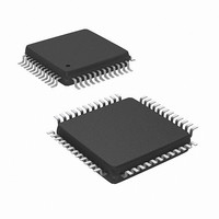
NuMicro M051 Series Technical Reference Manual 48-pin LQFP, 33-pin QFN - 16 - Publication Release Date: Sep 14, 2010 Revision V1.2 ...
Page 17
NuMicro M051 Series Technical Reference Manual 3 BLOCK DIAGRAM Figure 5.1-1 NuMicro™ M051 Series Block Diagram Publication Release Date: Sept 14, 2010 - 17 - Revision V1.2 ...
Page 18
... NuMicro M051 4 SELECTION TABLE NuMicro M051™ Series Selection Guide APRO Data Part No. RAM M Flash 8KB 4KB 4KB M052LAN 8KB 4KB 4KB M052ZAN 16KB 4KB 4KB M054LAN 16KB 4KB 4KB M054ZAN 32KB 4KB 4KB M058LAN 32KB 4KB 4KB M058ZAN 64KB 4KB ...
Page 19
NuMicro M051 Series Technical Reference Manual CPU core ARM Cortex M0 Part Number Flash ROM 8K Flash ROM 54 : 16K Flash ROM 54 : 16K Flash ...
Page 20
NuMicro M051 5 PIN CONFIGURATION ™ Series Technical Reference Manual Publication Release Date: Sep 14, 2010 - 20 - Revision V1.2 ...
Page 21
NuMicro M051 Series Technical Reference Manual 5.1 QFN 33 pin Figure 5.1-1 NuMicro™ M051 Series QFN33 Pin Diagram Publication Release Date: Sept 14, 2010 - 21 - Revision V1.2 ...
Page 22
NuMicro M051 5.2 LQFP 48 pin Figure 5.2-1 NuMicro™ M051 Series LQFP-48 Pin Diagram ™ Series Technical Reference Manual Publication Release Date: Sep 14, 2010 - 22 - Revision V1.2 ...
Page 23
NuMicro M051 Series Technical Reference Manual 5.3 Pin Description Pin number Alternate Function Symbol QFN33 LQFP48 XTAL1 10 15 XTAL2 27 41 VDD 12 17 VSS AVDD 4 6 AVSS LDO_C 13 18 ...
Page 24
NuMicro M051 Pin number Alternate Function Symbol QFN33 LQFP48 P0.5 MOSI_1 AD5 22 33 P0.6 MISO_1 AD6 21 32 P0.7 SPICLK1 AD7 29 43 P1.0 T2 AIN0 NC 44 P1.1 T3 AIN1 30 45 P1.2 ...
Page 25
NuMicro M051 Series Technical Reference Manual Pin number Alternate Function Symbol QFN33 LQFP48 P3.1 TXD 6 8 P3.2 STADC INT P3.3 MCLK INT P3.4 T0 SDA 8 11 P3.5 T1 ...
Page 26
NuMicro M051 6 FUNCTIONAL DESCRIPTION 6.1 ARM® Cortex™-M0 Core ™ The Cortex -M0 processor is a configurable, multistage, 32-bit RISC processor. It has an AMBA AHB- Lite interface and includes an NVIC component. It also has optional hardware debug functionality. ...
Page 27
NuMicro M051 Series Technical Reference Manual The system interface supports little-endian data accesses. The ability to have deterministic, fixed-latency, interrupt handling. Load/store-multiples and multicycle-multiplies that can be abandoned and restarted to facilitate rapid interrupt handling. C Application Binary Interface ...
Page 28
NuMicro M051 6.2 System Manager 6.2.1 Overview The following functions are included in system manager section System Resets System Memory Map System management registers for Part Number ID, chip reset and on-chip module reset , multi-functional pin control System Timer ...
Page 29
NuMicro M051 Series Technical Reference Manual Digital power from VDD and VSS supplies the power to the internal regulator which provides a fixed 2.5V power for digital operation and I/O pins. The outputs of internal voltage regulator, which is ...
Page 30
NuMicro M051 6.2.4 Whole System Memory Map ™ NuMicro M051 series provides a 4G-byte address space. The memory locations assigned to each on-chip modules are shown in Table 6.2-1. The detailed register memory addressing and programming will be described in ...
Page 31
NuMicro M051 Series Technical Reference Manual 0x4004_0000 – 0x4004_3FFF PWMA_BA 0x4005_0000 – 0x4005_3FFF UART0_BA 0x400E_0000 – 0x400E_FFFF ADC_BA 0x4011_0000 – 0x4011_3FFF TMR23_BA 0x4014_0000 – 0x4014_3FFF PWMB_BA 0x4015_0000 – 0x4015_3FFF UART1_BA System Control Space (0xE000_E000 ~ 0xE000_EFFF) 0xE000_E010 – 0xE000_E0FF ...
Page 32
NuMicro M051 6.2.5 Whole System Memory Mapping Table M052/54/58/516 4 GB 0xFFFF_FFFF Reserved 0xE000_F000 0xE000_EFFF System Control 0xE000_E000 0xE000_E00F Reserved 0x6002_0000 0x6001_FFFF EBI 0x6000_0000 0x5FFF_FFFF Reserved 0x5020_0000 0x501F_FFFF AHB 0x5000_0000 0x4FFF_FFFF Reserved 0x4020_0000 0x401F_FFFF APB 1 GB 0x4000_0000 0x3FFF_FFFF Reserved ...
Page 33
NuMicro M051 Series Technical Reference Manual 6.2.6 System Manager Controller Registers Map Register Offset R/W GCR_BA = 0x5000_0000 GCR_BA+0x00 R PDID GCR_BA+0x04 R/W RSTSRC GCR_BA+0x08 R/W IPRSTC1 GCR_BA+0x0C R/W IPRSTC2 GCR_BA+0x18 R/W BODCR GCR_BA+0x24 R/W PORCR GCR_BA+0x30 R/W P0_MFP ...
Page 34
... Bits Descriptions Part Device Identification Number This register reflects device part number code. S/W can read this register to identify [31:0] PDID which device is used. For example, M052LAN PDID code is 0x0000_5200. ™ NuMicro M051 series M052LAN M054LAN M058LAN M0516LAN M052ZAN M054ZAN M058ZAN ™ ...
Page 35
NuMicro M051 Series Technical Reference Manual M0516ZAN 0x00005A03 Publication Release Date: Sept 14, 2010 - 35 - Revision V1.2 ...
Page 36
NuMicro M051 System Reset Source Register (RSTSRC) This register provides specific information for software to identify this chip’s reset source from last operation. Register Offset R/W GCR_BA+04 R/W RSTSRC ...
Page 37
NuMicro M051 Series Technical Reference Manual 0= No reset from MCU This bit is cleared by writing 1 to itself. The RSTS_BOD flag is set by the “reset signal” from the Brown-Out-Detector module to indicate the previous reset source. ...
Page 38
NuMicro M051 Peripheral Reset Control Register1 (IPRSTC1) Register Offset R/W GCR_BA+08 R/W IPRSTC1 Reserved Bits Descriptions [31:4] Reserved Reserved EBI Controller Reset Set these bit “1” will generate ...
Page 39
NuMicro M051 Series Technical Reference Manual REGWRPROT at address GCR_BA+0x100. 0= Normal 1= Reset CPU CHIP one shot reset. Set this bit will reset the CHIP, including CPU kernel and all peripherals, and this bit will automatically return to ...
Page 40
NuMicro M051 Peripheral Reset Control Register2 (IPRSTC2) Set these bit “1” will generate asynchronous reset signal to the correspond IP. User need to set bit to “0” to release IP from the reset state Register Offset R/W GCR_BA+0C R/W IPRSTC2 ...
Page 41
NuMicro M051 Series Technical Reference Manual 1= PWM0~3 controller reset [19:18] Reserved Reserved UART1 controller Reset [17] 0= UART1 controller normal operation UART1_RST 1= UART1 controller reset UART0 controller Reset [16] 0= UART0 controller normal operation UART0_RST 1= UART0 ...
Page 42
NuMicro M051 1= Timer0 controller reset GPIO (P0~P4) controller Reset [1] 0= GPIO controller normal operation GPIO_RST 1= GPIO controller reset [0] Reserved Reserved Series Technical Reference Manual Publication Release Date: Sep 14, 2010 - 42 - Revision V1.2 ...
Page 43
NuMicro M051 Series Technical Reference Manual Brown-Out Detector Control Register (BODCR) Partial of the BODCR control registers values are initiated by the flash configuration and write- protected. Programming these protected bits needs to write “59h”, “16h”, “88h” to address ...
Page 44
NuMicro M051 Brown Out Detector Low power Mode (write-protected bit) 1= Enable the BOD low power mode [5] BOD_LPM 0= BOD operate in normal mode (default) The BOD consumes about 100uA in normal mode, the low power mode can ...
Page 45
NuMicro M051 Series Technical Reference Manual Power-On-Reset Control Register (PORCR) Register Offset R/W PORCR GCR_BA+0x24 R Bits Descriptions [31:16] Reserved Reserved The register is used for the ...
Page 46
NuMicro M051 Multiple Function Port0 Control Register (P0_MFP) Register Offset R/W GCR_BA+30 R/W P0_MFP Bits Descriptions [31:24] Reserved Reserved P0[7:0] input Schmitt Trigger function Enable [23:16] 1= P0[7:0] ...
Page 47
NuMicro M051 Series Technical Reference Manual P0.6 alternate function Selection The pin function of P0.6 depends on P0_MFP[6] and P0_ALT[6]. P0_ALT[6] 0 [14] P0_ ALT[ P0.5 alternate function Selection The pin function of P0.5 is depend ...
Page 48
NuMicro M051 1 1 P0.2 alternate function Selection The pin function of P0.2 depends on P0_MFP[2] and P0_ALT[2]. P0_ALT[2] 0 [10] P0_ ALT[ P0.1 alternate function Selection The pin function of P0.1 depends on P0_MFP[1] and ...
Page 49
NuMicro M051 Series Technical Reference Manual Refer to P0_ALT for details descriptions. Publication Release Date: Sept 14, 2010 - 49 - Revision V1.2 ...
Page 50
NuMicro M051 Multiple Function Port1 Control Register (P1_MFP) Register Offset R/W GCR_BA+34 R/W P1_MFP Bits Descriptions [31:24] Reserved Reserved P1[7:0] input Schmitt Trigger function Enable [23:16] P1_TYPEn 1= ...
Page 51
NuMicro M051 Series Technical Reference Manual P1.6 alternate function Selection The pin function of P1.6 depends on P1_MFP[6] and P1_ALT[6]. P1_ALT[6] 0 [14] P1_ ALT[ P1.5 alternate function Selection The pin function of P1.5 depends on ...
Page 52
NuMicro M051 1 1 P1.2 alternate function Selection The pin function of P1.2 depends on P1_MFP[2] and P1_ALT[2]. P1_ALT[2] 0 [10] P1_ ALT[ P1.1 alternate function Selection The pin function of P1.1 depends on P1_MFP[1] and ...
Page 53
NuMicro M051 Series Technical Reference Manual Refer to P1_ALT for details descriptions. Publication Release Date: Sept 14, 2010 - 53 - Revision V1.2 ...
Page 54
NuMicro M051 Multiple Function Port2 Control Register (P2_MFP) Register Offset R/W GCR_BA+38 R/W P2_MFP Bits Descriptions [31:24] Reserved Reserved P2[7:0] input Schmitt Trigger function Enable [23:16] P2_TYPEn 1= ...
Page 55
NuMicro M051 Series Technical Reference Manual 1 P2.6 alternate function Selection The pin function of P2.6 depends on P2_MFP[6] and P2_ALT[6]. P2_ALT[6] 0 [14] P2_ ALT[ P2.5 alternate function Selection The pin function of P2.5 depends ...
Page 56
NuMicro M051 P2_ALT[ P2.2 alternate function Selection The pin function of P2.2 depends on P2_MFP[2] and P2_ALT[2]. P2_ALT[2] 0 [10] P2_ ALT[ P2.1 alternate function Selection The pin function of P2.1 depends ...
Page 57
NuMicro M051 Series Technical Reference Manual multiple function Selection [7:0] P2_MFP[7:0] The pin function of P2 depends on P2_MFP and P2_ALT. Refer to P2_ALT for details descriptions. 0 PWM0(PWM generator 0) 1 Reserved Publication Release Date: ...
Page 58
NuMicro M051 Multiple Function Port3 Control Register (P3_MFP) Register Offset R/W GCR_BA+3C R/W P3_MFP Bits Descriptions [31:24] Reserved Reserved P3[7:0] input Schmitt Trigger function Enable [23:16] P3_TYPEn 1= ...
Page 59
NuMicro M051 Series Technical Reference Manual P3_ALT[ P3.5 alternate function Selection The pin function of P3.5 depends on P3_MFP[5] and P3_ALT[5]. P3_ALT[5] 0 [13] P3_ ALT[ P3.4 alternate function Selection The pin ...
Page 60
NuMicro M051 P3.2 alternate function Selection The pin function of P3.2 depends on P3_MFP[2] and P3_ALT[2]. P3_ALT[2] [10] P3_ ALT[ P3.1 alternate function Selection The pin function of P3.1 depends on P3_MFP[1] and P3_ALT[1]. P3_ALT[1] [9] ...
Page 61
NuMicro M051 Series Technical Reference Manual Multiple Function Port4 Control Register (P4_MFP) Register Offset R/W GCR_BA+40 R/W P4_MFP Bits Descriptions [31:24] Reserved Reserved P4[7:0] input Schmitt Trigger ...
Page 62
NuMicro M051 The pin function of P4.6 depends on P4_MFP[6] and P4_ALT[6]. P4_ALT[ P4.5 alternate function Selection The pin function of P4.5 depends on P4_MFP[5] and P4_ALT[5]. P4_ALT[5] [13] P4_ ALT[ P4.4 alternate ...
Page 63
NuMicro M051 Series Technical Reference Manual P4_ALT[ P4.1 alternate function Selection The pin function of P4.1 depends on P4_MFP[1] and P4_ALT[1]. P4_ALT[1] [9] P4_ ALT[ P4.0 alternate function Selection The pin function of ...
Page 64
NuMicro M051 Register Write-Protection Control Register (REGWRPROT) Some of the system control registers need to be protected to avoid inadvertent write and disturb the chip operation. These system control registers are protected after the power on reset till user to ...
Page 65
NuMicro M051 Series Technical Reference Manual [31:16] Reserved Reserved Register Write-Protected Code (Write Only) REGWRPRO Some write-protected registers have to be disabled the protected function by writing the [7:0] T sequence value “59h”, “16h”, “88h” to this field. After ...
Page 66
NuMicro M051 6.2.7 System Timer (SysTick) The Cortex-M0 includes an integrated system timer, SysTick. SysTick provides a simple, 24-bit clear-on-write, decrementing, wrap-on-zero counter with a flexible control mechanism. The counter can be used as a Real Time Operating System (RTOS) ...
Page 67
NuMicro M051 Series Technical Reference Manual 6.2.7.1 System Timer Control Register Map R: read only, W: write only, R/W: both read and write Register Offset R/W SCS_BA = 0xE000_E000 SCS_BA+010 R/W SYST_CSR SCS_BA+014 R/W SYST_RVR SCS_BA+018 R/W SYST_CVR SysTick ...
Page 68
NuMicro M051 Returns 1 if timer counted to 0 since last time this register was read. [16] COUNTFLAG is set by a count transition from COUNTFLAG COUNTFLAG is cleared on read write to the ...
Page 69
NuMicro M051 Series Technical Reference Manual Bits Descriptions [31:24] Reserved Reserved [23:0] Value to load into the Current Value register when the counter reaches 0. RELOAD SysTick Current Value Register (SYST_CVR) Register Offset R/W SCS_BA+ 018 R/W SYST_CVR 31 ...
Page 70
NuMicro M051 6.2.8 Nested Vectored Interrupt Controller (NVIC) Cortex-M0 provides an interrupt controller as an integral part of the exception mode, named as “Nested Vectored Interrupt Controller (NVIC)” closely coupled to the processor kernel and provides following features: ...
Page 71
NuMicro M051 Series Technical Reference Manual 6.2.8.1 Exception Model and System Interrupt Map The Table 6.2-2 lists the exception model supported by NuMicro M051 four levels of priority on some of these exceptions as well as on all interrupts. ...
Page 72
NuMicro M051 Series Technical Reference Manual 29 0x74 13 UART1_INT 30 0x78 14 SPI0_INT 31 0x7C 15 SPI1_INT 32-33 0x80-0x84 16- 0x88 18 I2C_INT 0x8C- 35-43 19-27 - 0xAC 44 0xB0 28 PWRWU_INT 45 0xB4 29 ADC_INT ...
Page 73
NuMicro M051 Series Technical Reference Manual 6.2.8.2 Vector Table When any interrupts is accepted, the processor will automatically fetch the starting address of the interrupt service routine (ISR) from a vector table in memory. For ARMv6-M, the vector table ...
Page 74
NuMicro M051 6.2.8.3 Operation Description NVIC interrupts can be enabled and disabled by writing to their corresponding Interrupt Set- Enable or Interrupt Clear-Enable register bit-field. The registers use a write-1-to-enable and write- 1-to-clear policy, both registers reading back the current ...
Page 75
NuMicro M051 Series Technical Reference Manual SCS_BA+410 R/W NVIC_IPR4 SCS_BA+414 R/W NVIC_IPR5 SCS_BA+418 R/W NVIC_IPR6 SCS_BA+41C R/W NVIC_IPR7 IRQ0 ~ IRQ31 Set-Enable Control Register (NVIC_ISER) Register Offset R/W SCS_BA+100 R/W NVIC_ISER ...
Page 76
NuMicro M051 IRQ0 ~ IRQ31 Clear-Enable Control Register (NVIC_ICER) Register Offset R/W SCS_BA+180 R/W NVIC_ICER Bits Descriptions Disable one or more interrupts within a group of 32. Each ...
Page 77
NuMicro M051 Series Technical Reference Manual IRQ0 ~ IRQ31 Set-Pending Control Register (NVIC_ISPR) Register Offset R/W SCS_BA+200 R/W NVIC_ISPR Bits Descriptions Writing bit pends ...
Page 78
NuMicro M051 IRQ0 ~ IRQ31 Clear-Pending Control Register (NVIC_ICPR) Register Offset R/W SCS_BA+280 R/W NVIC_ICPR Bits Descriptions Writing bit un-pends the associated interrupt under software ...
Page 79
NuMicro M051 Series Technical Reference Manual IRQ0 ~ IRQ3 Interrupt Priority Register (NVIC_IPR0) Register Offset R/W SCS_BA+400 R/W NVIC_IPR0 PRI_3 PRI_2 PRI_1 PRI_0 Bits Descriptions Priority of ...
Page 80
NuMicro M051 IRQ4 ~ IRQ7 Interrupt Priority Register (NVIC_IPR1) Register Offset R/W SCS_BA+404 R/W NVIC_IPR1 PRI_7 PRI_6 PRI_5 PRI_4 Bits Descriptions Priority of IRQ7 [31:30] PRI_7 “0” denotes ...
Page 81
NuMicro M051 Series Technical Reference Manual IRQ8 ~ IRQ11 Interrupt Priority Register (NVIC_IPR2) Register Offset R/W SCS_BA+408 R/W NVIC_IPR2 PRI_11 PRI_10 PRI_9 PRI_8 Bits Descriptions Priority of ...
Page 82
NuMicro M051 IRQ12 ~ IRQ15 Interrupt Priority Register (NVIC_IPR3) Register Offset R/W SCS_BA+40C R/W NVIC_IPR3 PRI_15 PRI_14 PRI_13 PRI_12 Bits Descriptions Priority of IRQ15 [31:30] PRI_15 “0” denotes ...
Page 83
NuMicro M051 Series Technical Reference Manual IRQ16 ~ IRQ19 Interrupt Priority Register (NVIC_IPR4) Register Offset R/W SCS_BA+ 410 R/W NVIC_IPR4 PRI_19 PRI_18 PRI_17 PRI_16 Bits Descriptions Priority ...
Page 84
NuMicro M051 IRQ20 ~ IRQ23 Interrupt Priority Register (NVIC_IPR5) Register Offset R/W SCS _BA + NVIC_IPR R/W 414 PRI_23 PRI_22 PRI_21 PRI_20 Bits Descriptions Priority of IRQ23 ...
Page 85
NuMicro M051 Series Technical Reference Manual IRQ24 ~ IRQ27 Interrupt Priority Register (NVIC_IPR6) Register Offset R/W NVIC_IPR SCS_BA+418 R PRI_27 PRI_26 PRI_25 PRI_24 Bits Descriptions Priority ...
Page 86
NuMicro M051 IRQ28 ~ IRQ31 Interrupt Priority Register (NVIC_IPR7) Register Offset R/W SCS_BA+41C R/W NVIC_IPR7 PRI_31 PRI_30 PRI_29 PRI_28 Bits Descriptions Priority of IRQ31 [31:30] PRI_31 “0” denotes ...
Page 87
NuMicro M051 Series Technical Reference Manual 6.2.8.5 Interrupt Source Control Registers Besides the interrupt control registers associated with the NVIC, NuMicro M051 implement some specific control registers to facilitate the interrupt functions, including “interrupt source identify”, ”NMI source selection” ...
Page 88
NuMicro M051 INT_BA+0x3C R IRQ15_SRC INT_BA+0x40 Reserved IRQ16_SRC INT_BA+0x44 Reserved IRQ17_SRC INT_BA+0x48 R IRQ18_SRC INT_BA+0x4C Reserved IRQ19_SRC INT_BA+0x50 Reserved IRQ20_SRC INT_BA+0x54 Reserved IRQ21_SRC INT_BA+0x58 Reserved IRQ22_SRC INT_BA+0x5C Reserved IRQ23_SRC INT_BA+0x60 Reserved IRQ24_SRC INT_BA+0x64 Reserved IRQ25_SRC INT_BA+0x68 Reserved IRQ26_SRC INT_BA+0x6C ...
Page 89
NuMicro M051 Series Technical Reference Manual INT_BA+0x80 R/W NMI_SEL INT_BA+0x84 R/W MCU_IRQ NMI source interrupt select control register MCU IRQ Number identity register Publication Release Date: Sept 14, 2010 - 89 - 0x0000_0000 0x0000_0000 Revision V1.2 ...
Page 90
NuMicro M051 Interrupt Source Identity Register (IRQn_SRC) Register Offset R/W INT_BA+0x00 …….. R IRQn_SRC INT_BA+0x7C Reserved Address INT-Num Bits INT_BA+0x00 0 [2:0] INT_BA+0x04 1 [2:0] INT_BA+0x08 2 [2:0] ...
Page 91
NuMicro M051 Series Technical Reference Manual INT_BA+0x10 4 [2:0] INT_BA+0x14 5 [2:0] INT_BA+0x18 6 [3:0] INT_BA+0x1C 7 [3:0] INT_BA+0x20 8 [2:0] INT_BA+0x24 9 [2:0] INT_BA+0x28 10 [2:0] INT_BA+0x2C 11 [2:0] INT_BA+0x30 12 [2:0] Bit0: EINT1 – external interrupt 1 ...
Page 92
NuMicro M051 INT_BA+0x34 13 [2:0] INT_BA+0x38 14 [2:0] INT_BA+0x3C 15 [2:0] INT_BA+0x40 16 [2:0] INT_BA+0x44 17 [2:0] INT_BA+0x48 18 [2:0] INT_BA+0x4C 19 [2:0] INT_BA+0x50 20 [2:0] INT_BA+0x54 21 [2:0] INT_BA+0x58 22 [2:0] INT_BA+0x5C 23 [2:0] INT_BA+0x60 24 [2:0] INT_BA+0x64 ...
Page 93
NuMicro M051 Series Technical Reference Manual INT_BA+0x74 29 [2:0] INT_BA+0x78 30 [2:0] INT_BA+0x7C 31 [2:0] Bit0: PWRWU_INT Bit2 = 0 Bit1 = 0 Bit0: ADC_INT Reserved Reserved Publication Release Date: Sept 14, 2010 - 93 - Revision V1.2 ...
Page 94
NuMicro M051 NMI Interrupt Source Select Control Register (NMI_SEL) Register Offset R/W INT_BA+0x80 R/W NMI_SEL Reserved Bits Descriptions Reserved [31:5] Reserved The NMI interrupt to Cortex-M0 can be ...
Page 95
NuMicro M051 Series Technical Reference Manual MCU Interrupt Request Source Register (MCU_IRQ) Register Offset R/W INT_BA+0x84 R/W MCU_IRQ Bits Descriptions MCU IRQ Source Register The MCU_IRQ collects ...
Page 96
NuMicro M051 6.2.9 System Controller Registers Map Cortex-M0 status and operating mode control are managed System Control Registers. Including CPUID, Cortex-M0 interrupt priority and Cortex-M0power management can be controlled through these system control register For more detailed information, please refer ...
Page 97
NuMicro M051 Series Technical Reference Manual CPUID Base Register (CPUID) Register Offset R/W SCS_BA + R CPUID 0xD00 Reserved PARTNO[3:0] Bits Descriptions [31:24] Implementer code assigned by ...
Page 98
NuMicro M051 Interrupt Control State Register (ICSR) Register Offset R/W SCS_BA + R/W ICSR 0xD04 NMIPENDS Reserved ISRPREEMP ISRPENDIN Reserved VECTPENDING[3: Bits R/W Descriptions [31] ...
Page 99
NuMicro M051 Series Technical Reference Manual [23] R ISRPREEMPT [22] R ISRPENDING [20:12] R VECTPENDING [8:0] R VECTACTIVE Application Interrupt and Reset Control Register (AIRCR) Register Offset R/W SCS_BA+0xD0C R/W AIRCR ...
Page 100
NuMicro M051 [15:3] Reserved Reserved Writing this bit 1 will cause a reset signal to be asserted to the chip to indicate a reset is requested. [2] SYSRESETREQ The bit is a write only bit and self-clears as part ...
Page 101
NuMicro M051 Series Technical Reference Manual System Control Register (SCR) Register Offset R/W SCS_BA+0xD10 R/W SCR Reserved Bits Descriptions When enabled, interrupt transitions from Inactive to Pending ...
Page 102
NuMicro M051 System Handler Priority Register 2 (SHPR2) Register Offset R/W SCS_BA + SHPR2 R/W 0xD1C PRI_11 Bits Descriptions Priority of system handler 11 – SVCall [31:30] PRI_11 ...
Page 103
NuMicro M051 Series Technical Reference Manual System Handler Priority Register 3 (SHPR3) Register Offset R/W SCS_BA + SHPR3 R/W 0xD20 PRI_15 PRI_14 Bits Descriptions Priority of system ...
Page 104
NuMicro M051 6.3 Clock Controller 6.3.1 Overview The clock controller generates the clocks for the whole chip, including system clocks and all peripheral clocks. The clock controller also implements the power control function with the individually clock ON/OFF control, clock ...
Page 105
NuMicro M051 Series Technical Reference Manual XTL12M_EN(PWRCON[ 0]) XT_IN 4~24M External Crystal XT_OUT OSC22M_EN(PWRCON[ 2]) 22.1184 Internal OSC22M OSC10K_EN(PWRCON[ 3]) 10K OSC10K Figure 6.3-1 Clock generator block diagram PLL_SRC(PLLCON[19]) 1 PLL 0 M Publication Release Date: Sept 14, 2010 ...
Page 106
NuMicro M051 6.3.3 System Clock & SysTick Clock The system clock has 4 clock sources which were generated from clock generator block. The clock source switch depends on the register HCLK_S(CLKSEL0[2:0]). The block diagram is shown in the Figure 6.3-2. ...
Page 107
NuMicro M051 Series Technical Reference Manual 6.3.4 AHB Clock Source Select HCLK EBI_EN (AHBCLK[3]) HCLK ISP_EN (AHBCLK[2]) Figure 6.3-4 AHB Clock Source for HCLK EBI (External Bus Interface) ISP (In System Programmer) Publication Release Date: Sept 14, 2010 - ...
Page 108
NuMicro M051 6.3.5 Peripherals Clock Source Select The peripherals clock had different clock source switch setting which depends on the different peripheral. Please refer the CLKSEL1 & APBCLK register description in chapter 6.3. ...
Page 109
NuMicro M051 Series Technical Reference Manual Figure 6.3-5 Peripherals Clock Source Select for PCLK Publication Release Date: Sept 14, 2010 - 109 - Revision V1.2 ...
Page 110
NuMicro M051 6.3.6 Power Down Mode (Deep Sleep Mode) Clock When chip enter into power down mode, most of clock sources, peripheral clocks and system clock will be disabled. Some of clock sources and peripherals clock are still active in ...
Page 111
NuMicro M051 Series Technical Reference Manual 6.3.7 Frequency Divider Output This device is equipped a power-of-2 frequency divider which is composed by16 chained divide- by-2 shift registers. One of the 16 shift register outputs selected by a sixteen to ...
Page 112
NuMicro M051 6.3.8 Clock Controller Registers Map R: read only, W: write only Register Offset R/W CLK_BA + 00 R/W PWRCON CLK_BA + 04 R/W AHBCLK CLK_BA + 08 R/W APBCLK CLKSTATUS CLK_BA + 0C R/W CLK_BA + 10 R/W ...
Page 113
NuMicro M051 Series Technical Reference Manual 6.3.9 Clock Controller Registers Description Power Down Control Register (PWRCON) All bits except bit6 (PD_WU_STS) are protected. Programming these protected bits needs to write “59h”, “16h”, “88h” to address 0x5000_0100 to disable register ...
Page 114
NuMicro M051 the PWR_DOWN_EN bit set. (b) if the PD_WAIT_CPU is “1”, then the chip keeps active till the CPU sleep mode is also active and then the chip enters power down mode When chip wakes up from power ...
Page 115
NuMicro M051 Series Technical Reference Manual The bit default value is set by flash controller user configuration register config0 [26:24]. When the default clock source is from external crystal, the bit is automatically set to “1” Crystal ...
Page 116
NuMicro M051 Register PWR_DOWN_EN PD_WAIT_CPU Instruction Mode 0 Normal Running Mode 0 IDLE Mode (CPU entry Sleep Mode) 1 Power_down Mode 1 Power_down Mode (CPU entry deep sleep mode) Table 6.3-1 Power Down Mode Control Table Series Technical Reference ...
Page 117
NuMicro M051 Series Technical Reference Manual AHB Devices Clock Enable Control Register (AHBCLK) These bits for AHBCLK register are used to enable/disable system and AHB engine clock. Register Offset R/W AHBCLK CLK_BA + 04 R ...
Page 118
NuMicro M051 APB Devices Clock Enable Control Register (APBCLK) These bits of APBCLK register are used to enable/disable clock for APB engine and peripherals. Register Offset R/W APBCLK CLK_BA Reserved PWM67_EN PWM45_EN ...
Page 119
NuMicro M051 Series Technical Reference Manual 0 = Disable PWM45 clock PWM_23 Clock Enable [21 Enable PWM23 clock PWM23_EN 0 = Disable PWM23 clock PWM_01 Clock Enable [20 Enable PWM01 clock PWM01_EN 0 = Disable ...
Page 120
NuMicro M051 Timer3 Clock Enable [ Enable Timer3 Clock TMR3_EN 0 = Disable Timer3 Clock Timer2 Clock Enable [ Enable Timer2 Clock TMR2_EN 0 = Disable Timer2 Clock Timer1 Clock Enable [ Enable ...
Page 121
NuMicro M051 Series Technical Reference Manual Clock status Register (CLKSTATUS) These bits of this register are used to monitor if the chip clock source stable or not, and if clock switching failed. Register Offset R/W CLKSTATUS CLK_BA+0C R/W 31 ...
Page 122
NuMicro M051 OSC10K clock source stable flag (Read Only) [ OSC10K clock is stable OSC10K_STB 0 = OSC10K clock is not stable or disable PLL clock source stable flag (Read Only) [ PLL clock is ...
Page 123
NuMicro M051 Series Technical Reference Manual Clock Source Select Control Register 0 (CLKSEL0) Register Offset R/W [1] CLK_BA + 10 R/W CLKSEL0 Reserved Bits Descriptions [31:6] Reserved ...
Page 124
NuMicro M051 Series Technical Reference Manual 2. The 3-bit default value is reloaded from the value of CFOSC (Config0[26:24]) in user configuration register of Flash controller by any reset. Therefore the default value is either 000b or 111b. 3. ...
Page 125
NuMicro M051 Series Technical Reference Manual Clock Source Select Control Register 1(CLKSEL1) Before clock switching the related clock sources (current and new) must be turned on. Register Offset R/W CLK_BA + 14 R/W CLKSEL1 PWM23_S 23 ...
Page 126
NuMicro M051 10 = Clock source from HCLK 11 = Clock source from internal 22.1184 MHz oscillator clock [27:26] Reserved Reserved UART clock source select Clock source from external crystal clock (4 ~ 24MHz) [25:24] UART_S 01 ...
Page 127
NuMicro M051 Series Technical Reference Manual TIMER0 clock source select. 000 = Clock source from external crystal clock ( MHz) 001 = Reserved [10:8] TMR0_S 010 = Clock source from HCLK 011 = Clock source from external ...
Page 128
NuMicro M051 Clock Source Select Control Register (CLKSEL2) Before clock switching the related clock sources (pre-select and new-select) must be turned on. Register Offset R/W CLK_BA + 1C R/W CLKSEL2 ...
Page 129
NuMicro M051 Series Technical Reference Manual 00 = Clock source from external crystal clock ( MHz Reserved 10 = Clock source from HCLK 11 = Clock source from internal 22.1184 MHz oscillator clock Clock Divider ...
Page 130
NuMicro M051 Clock Divider Register (CLKDIV) Register Offset R/W CLK_BA_+ 18 R/W CLKDIV Reserved Reserved Bits Descriptions [31:24] Reserved Reserved ADC clock divide number from ADC clock source ...
Page 131
NuMicro M051 Series Technical Reference Manual PLL Control Register (PLLCON) The PLL reference clock input is from the external crystal clock input internal 22.1184 MHz oscillator. This register is used to control the PLL output frequency and PLL operating ...
Page 132
NuMicro M051 Power Down Mode. If set the IDLE bit “1” in PWRCON register, the PLL will enter power down mode too [16 PLL is in normal mode (default PLL is in power-down mode ...
Page 133
NuMicro M051 Series Technical Reference Manual PLL Output Clock Frequency Setting × × FOUT FIN NR NO Constrain: < < 1. 3.2MHz FIN 150MHz FIN < < 2. 800KHz 8MHz FIN < < ...
Page 134
NuMicro M051 Frequency Divider Control Register (FRQDIV) Register Offset R/W CLK_BA+ 24 R/W FRQDIV Reserved Bits Descriptions [31:5] Reserved Reserved Frequency Divider Enable Bit [ Disable ...
Page 135
NuMicro M051 Series Technical Reference Manual 6.4 General Purpose I/O 6.4.1 Overview There are 40 General Purpose I/O pins shared with special feature functions in this MCU. The 40 pins are arranged in 5 ports named with P0, P1, ...
Page 136
NuMicro M051 6.4.1.3 Open-Drain Mode Explanation (PMDn[1:0]) to 2’b10 the Px[n] pin is in Open-Drain mode and the I/O pin supports Set Px_PMD digital output function but only with sink current capability, an additional pull-up resister is needed for driving ...
Page 137
NuMicro M051 Series Technical Reference Manual 2 CPU Clock Delay Port Latch Data Figure 6.4-3 Quasi-bidirectional I/O Mode VDD Very Strong Weak N Input Data Publication Release Date: Sept 14, 2010 - 137 - Weak Port ...
Page 138
NuMicro M051 6.4.2 Port 0-4 Controller Registers Map R: read only, W: write only, R/W: both read and write Register Offset GP_BA = 0x5000_4000 GP_BA+0x000 P0_PMD GP_BA+0x004 P0_OFFD GP_BA+0x008 P0_DOUT GP_BA+0x00C P0_DMASK GP_BA+0x010 P0_PIN GP_BA+0x014 P0_DBEN GP_BA+0x018 P0_IMD GP_BA+0x01C P0_IEN ...
Page 139
NuMicro M051 Series Technical Reference Manual GP_BA+0x088 P2_DOUT GP_BA+0x08C P2_DMASK GP_BA+0x090 P2_PIN GP_BA+0x094 P2_DBEN GP_BA+0x098 P2_IMD GP_BA+0x09C P2_IEN GP_BA+0x0A0 P2_ISRC GP_BA+0x0C0 P3_PMD GP_BA+0x0C4 P3_OFFD GP_BA+0x0C8 P3_DOUT GP_BA+0x0CC P3_DMASK GP_BA+0x0D0 P3_PIN GP_BA+0x0D4 P3_DBEN GP_BA+0x0D8 P3_IMD GP_BA+0x0DC P3_IEN GP_BA+0x0E0 P3_ISRC GP_BA+0x100 ...
Page 140
NuMicro M051 GP_BA+0x180 R/W DBNCECON GP_BA+0x200 R/W P00_DOUT GP_BA+0x204 R/W P01_DOUT GP_BA+0x208 R/W P02_DOUT GP_BA+0x20C R/W P03_DOUT GP_BA+0x210 R/W P04_DOUT GP_BA+0x214 R/W P05_DOUT GP_BA+0x218 R/W P06_DOUT GP_BA+0x21C R/W P07_DOUT GP_BA+0x220 R/W P10_DOUT GP_BA+0x224 R/W P11_DOUT GP_BA+0x228 R/W P12_DOUT GP_BA+0x22C ...
Page 141
NuMicro M051 Series Technical Reference Manual GP_BA+0x25C P27_DOUT GP_BA+0x260 P30_DOUT GP_BA+0x264 P31_DOUT GP_BA+0x268 P32_DOUT GP_BA+0x26C P33_DOUT GP_BA+0x270 P34_DOUT GP_BA+0x274 P35_DOUT GP_BA+0x278 P36_DOUT GP_BA+0x27C P37_DOUT GP_BA+0x280 P40_DOUT GP_BA+0x284 P41_DOUT GP_BA+0x288 P42_DOUT GP_BA+0x28C P43_DOUT GP_BA+0x290 P44_DOUT GP_BA+0x294 P45_DOUT GP_BA+0x298 P46_DOUT GP_BA+0x29C ...
Page 142
NuMicro M051 6.4.3 Port 0-4 Controller Registers Description Port 0-4 I/O Mode Control (Px_PMD) Register Offset R/W GP_BA+0x000 R/W P0_PMD GP_BA+0x040 R/W P1_PMD GP_BA+0x080 R/W P2_PMD GP_BA+0x0C0 R/W P3_PMD GP_BA+0x100 R/W P4_PMD ...
Page 143
NuMicro M051 Series Technical Reference Manual x=0~ 0~7 Publication Release Date: Sept 14, 2010 - 143 - Revision V1.2 ...
Page 144
NuMicro M051 Port 0-4 Bit OFF Digital Resistor Enable (Px_OFFD) Register Offset R/W GP_BA+0x004 R/W P0_OFFD GP_BA+0x044 R/W P1_OFFD GP_BA+0x084 R/W P2_OFFD GP_BA+0x0C4 R/W P3_OFFD GP_BA+0x104 R/W P4_OFFD ...
Page 145
NuMicro M051 Series Technical Reference Manual Port 0-4 Data Output Value (Px_DOUT) Register Offset R/W GP_BA+0x008 R/W P0_DOUT GP_BA+0x048 R/W P1_DOUT GP_BA+0x088 R/W P2_DOUT GP_BA+0x0C8 R/W P3_DOUT GP_BA+0x108 R/W P4_DOUT ...
Page 146
NuMicro M051 Port0-4 Data Output Write Mask (Px _DMASK) Register Offset R/W P0_DMASK GP_BA+0x00C R/W P1_DMASK GP_BA+0x04C R/W P2_DMASK GP_BA+0x08C R/W P3_DMASK GP_BA+0x0CC R/W P4_DMASK GP_BA+0x10C R Bits ...
Page 147
NuMicro M051 Series Technical Reference Manual Port 0-4 Pin Value (Px _PIN) Register Offset R/W GP_BA+0x010 R P0_PIN GP_BA+0x050 R P1_PIN GP_BA+0x090 R P2_PIN GP_BA+0x0D0 R P3_PIN GP_BA+0x110 R P4_PIN ...
Page 148
NuMicro M051 Port 0-4 De-bounce Enable (Px _DBEN) Register Offset R/W GP_BA+0x014 R/W P0_DBEN GP_BA+0x054 R/W P1_DBEN GP_BA+0x094 R/W P2_DBEN GP_BA+0x0D4 R/W P3_DBEN GP_BA+0x114 R/W P4_DBEN Bits Descriptions ...
Page 149
NuMicro M051 Series Technical Reference Manual x=0~ 0~7 Publication Release Date: Sept 14, 2010 - 149 - Revision V1.2 ...
Page 150
NuMicro M051 Port 0-4 Interrupt Mode Control (Px _IMD) Register Offset R/W GP_BA+0x018 R/W P0_IMD GP_BA+0x058 R/W P1_IMD GP_BA+0x098 R/W P2_IMD GP_BA+0x0D8 R/W P3_IMD GP_BA+0x118 R/W P4_IMD Bits ...
Page 151
NuMicro M051 Series Technical Reference Manual x=0~ 0~7 Publication Release Date: Sept 14, 2010 - 151 - Revision V1.2 ...
Page 152
NuMicro M051 Port 0-4 Interrupt Enable Control (Px _IEN) Register Offset R/W GP_BA+0x01C R/W P0_IEN GP_BA+0x05C R/W P1_IEN GP_BA+0x09C R/W P2_IEN GP_BA+0x0DC R/W P3_IEN GP_BA+0x11C R/W P4_IEN Bits ...
Page 153
NuMicro M051 Series Technical Reference Manual x=0~ 0~7 Reserved [15:8] Reserved Port 0-4 Interrupt Enable by Input Falling Edge or Input Level Low IF_EN[n] used to enable the interrupt for each of the corresponding input Px[n]. Set ...
Page 154
NuMicro M051 Port 0-4 Interrupt Trigger Source (Px _ISRC) Register Offset R/W GP_BA+0x020 R/WC P0_ISRC GP_BA+0x060 R/WC P1_ISRC GP_BA+0x0A0 R/WC P2_ISRC GP_BA+0x0E0 R/WC P3_ISRC GP_BA+0x120 R/WC P4_ISRC Bits ...
Page 155
NuMicro M051 Series Technical Reference Manual Interrupt De-bounce Cycle Control (DBNCECON) Register Offset R/W DBNCECON GP_BA+0x180 R Reserved ICLK_ON Bits Descriptions Interrupt clock On mode Set this ...
Page 156
NuMicro M051 Series Technical Reference Manual 3 Sample interrupt input once per 8 clocks 4 Sample interrupt input once per 16 clocks 5 Sample interrupt input once per 32 clocks 6 Sample interrupt input once per 64 clocks 7 ...
Page 157
NuMicro M051 Series Technical Reference Manual GPIO Port [P0/P1/P2/P3/P4] I/O Bit Output Control (Pxx_DOUT) Register Offset R/W GP_BA+0x200 - R/W P0x_DOUT GP_BA+0x21C GP_BA+0x220 - R/W P1x_DOUT GP_BA+0x23C GP_BA+0x240 - R/W P2x_DOUT GP_BA+0x25C GP_BA+0x260 - R/W P3x_DOUT GP_BA+0x27C GP_BA+0x280 - ...
Page 158
NuMicro M051 Pxx I/O Pin Bit Output Control Set this bit can control one GPIO pin output value [0] Pxx_DOUT 1 = set corresponding GPIO bit to high 0 = set corresponding GPIO bit to low Series Technical Reference ...
Page 159
NuMicro M051 Series Technical Reference Manual 6.5 I2C Serial Interface Controller (Master/Slave) 6.5.1 Overview I2C is a two-wire, bi-directional serial bus that provides a simple and efficient method of data exchange between devices. The I2C standard is a true ...
Page 160
NuMicro M051 Serial clock synchronization allows devices with different bit rates to communicate via one serial bus Serial clock synchronization can be used as a handshake mechanism to suspend and resume serial transfer Built-in a 14-bit time-out counter will request ...
Page 161
NuMicro M051 Series Technical Reference Manual 6.5.3.2 Data transfer on the I2C-bus A master-transmitter addressing a slave receiver with a 7-bit address The transfer direction is not changed Figure 6.5-3 Master Transmits Data to Slave A master reads a ...
Page 162
NuMicro M051 usually referred to as the P-bit, is defined as a LOW to HIGH transition on the SDA line while SCL is HIGH. Figure 6.5-5 START and STOP condition 6.5.3.4 Slave Address Transfer The first byte of data transferred ...
Page 163
NuMicro M051 Series Technical Reference Manual Figure 6.5-6 Bit Transfer on the I2C bus Figure 6.5-7 Acknowledge on the I2C bus Publication Release Date: Sept 14, 2010 - 163 - Revision V1.2 ...
Page 164
NuMicro M051 6.5.4 I2C Protocol Registers The CPU interfaces to the SIO port through the following thirteen special function registers: I2CON (control register), I2CSTATUS (status register), I2CDAT (data register), I2CADDRn (address registers, n=0~3), I2CADMn (address mask registers, n=0~3), I2CLK (clock ...
Page 165
NuMicro M051 Series Technical Reference Manual by the I2C hardware and cannot be accessed by the CPU. Serial data is shifted through the acknowledge bit into I2CDAT [7:0] on the rising edges of serial clock pulses on the SCL ...
Page 166
NuMicro M051 6.5.4.4 Status Register (I2CSTATUS) I2CSTATUS [7: 8-bit read-only register. The three least significant bits are always 0. The bit field I2CSTATUS [7:3] contain the status code. There are 26 possible status codes, All states are listed ...
Page 167
NuMicro M051 Series Technical Reference Manual 0 Pclk Enable 1 1/4 DIV4 ENS1 ENTI SI Figure 6.5-9: I2C Time-out Count Block Diagram 14-bits Counter TIF Clear Counter SI Publication Release Date: Sept 14, 2010 - 167 - To I2C ...
Page 168
NuMicro M051 6.5.5 I2C Controller Registers Map R : read only write only, R/W : both read and write Register Offset R/W I2C_BA = 0x4002_0000 I2C_BA+0x00 R/W I2CON I2C_BA+0x04 R/W I2CADRR0 I2C_BA+0x08 R/W I2CDAT I2C_BA+0x0C R I2CSTATUS I2C_BA+0x10 ...
Page 169
NuMicro M051 Series Technical Reference Manual 6.5.6 I2C Controller Registers Description I2C CONTROL REGISTER (I2CON) Register Offset R/W Description I2C_BA+0x00 R/W I2C Control Register I2CON ENSI ...
Page 170
NuMicro M051 I2C STOP Control Bit In master mode, setting STO to transmit a STOP condition to bus then I2C hardware will check the bus condition if a STOP condition is detected this [4] STO bit will be cleared ...
Page 171
NuMicro M051 Series Technical Reference Manual I2C DATA REGISTER (I2CDAT) Register Offset R/W Description I2C_BA+0x08 R/W I2C DATA Register I2CDAT Bits Descriptions [31:8] Reserved Reserved I2C Data ...
Page 172
NuMicro M051 I2C STATUS REGISTER (I2CSTATUS ) Register Offset R/W Description I2CSTATUS I2C_BA+0x0C R/W I2C STATUS Register Bits Descriptions [31:8] Reserved Reserved I2C Status Register The status register ...
Page 173
NuMicro M051 Series Technical Reference Manual I2C BAUD RATE CONTROL REGISTER (I2CLK) Register Offset R/W Description I2C_BA+0x10 R/W I2C clock divided Register I2CLK Bits Descriptions [31:8] Reserved ...
Page 174
NuMicro M051 I2C TIME-OUT COUNTER REGISTER (I2CTOC) Register Offset R/W Description I2C_BA+0x14 R/W I2C Time-Out Counter Register I2CTOC Reserved Bits Descriptions [31:3] Reserved Reserved Time-out counter is enabled/disable ...
Page 175
NuMicro M051 Series Technical Reference Manual I2C SLAVE ADDRESS REGISTER (I2CADDRx) Register Offset R/W Description I2CADDR0 I2C_BA+0x04 R/W I2C slave Address Register0 I2CADDR1 I2C_BA+0x18 R/W I2C slave Address Register1 I2CADDR2 I2C_BA+0x1C R/W I2C slave Address Register2 I2CADDR3 I2C_BA+0x20 R/W ...
Page 176
NuMicro M051 I2C SLAVE ADDRESS MASK REGISTER (I2CADMx) Register Offset R/W Description I2C_BA+0x24 R/W I2C slave Address Mask Register0 I2CADM0 I2C_BA+0x28 R/W I2C slave Address Mask Register1 I2CADM1 I2C_BA+0x2C R/W I2C slave Address Mask Register2 I2CADM2 I2C_BA+0x30 R/W I2C slave ...
Page 177
NuMicro M051 Series Technical Reference Manual 6.5.7 Modes of Operation The on-chip I2C ports support five operation modes, Master transmitter, Master receiver, Slave transmitter, Slave receiver, and GC call given application, I2C port may operate as a ...
Page 178
NuMicro M051 6.5.8 Data Transfer Flow in Five Operating Modes The five operating modes are: Master/Transmitter, Master/Receiver, Slave/Transmitter, Slave/Receiver and GC Call. Bits STA, STO and AA in I2CON register will determine the next state of the SIO hardware after ...
Page 179
NuMicro M051 Series Technical Reference Manual From Slave Mode (C) (STA,STO,SI,AA)=(0,0,1,X) (STA,STO,SI,AA)=(1,0,1,X) Data byte will be transmitted; A repeated START will be ACK will be received. transmitted; 10H 28H A repeated START has Data byte in S1DAT has been ...
Page 180
NuMicro M051 Series Technical Reference Manual - 180 - Publication Release Date: Sep 14, 2010 Revision V1.2 ...
Page 181
NuMicro M051 Series Technical Reference Manual Figure 6.5-12 Master Receiver Mode Publication Release Date: Sept 14, 2010 - 181 - Revision V1.2 ...
Page 182
NuMicro M051 Series Technical Reference Manual - 182 - Publication Release Date: Sep 14, 2010 Revision V1.2 ...
Page 183
NuMicro M051 Series Technical Reference Manual A8H Own SLA+R has been received; ACK has been return. B0H Arbitration lost SLA+R/W as master; Own SLA+R has been received; ACK has been return. (STA,STO,SI,AA)=(0,0,1,0) Last data byte will be transmitted; ACK ...
Page 184
NuMicro M051 60H Own SLA+W has been received; ACK has been return. 68H Arbitration lost SLA+R/W as master; Own SLA+W has been received; ACK has been return. (STA,STO,SI,AA)=(0,0,1,0) Data byte will be received; NOT ACK will be returned. 88H ...
Page 185
NuMicro M051 Series Technical Reference Manual 70H Reception of the general call address and one or more data bytes; ACK has been return. 78H Arbitration lost SLA+R/W as master; and address as SLA by general call; ACK has been ...
Page 186
NuMicro M051 6.6 PWM Generator and Capture Timer 6.6.1 Overview ™ NuMicro M051 series has 2 sets of PWM group supports 4 sets of PWM Generators which can be configured as 8 independent PWM outputs, PWM0~PWM7 complementary ...
Page 187
NuMicro M051 Series Technical Reference Manual programmable by setting CCR0.CFL_IE0[2]] (Falling latch Interrupt enable) to decide the condition of interrupt occur. Capture channel 1 has the same feature by setting CCR0.CRL_IE1[17] and CCR0.CFL_IE1[18]. And capture channel 0 to channel ...
Page 188
NuMicro M051 6.6.3 Block Diagram The Figure 6.6-1 illustrate the architecture of PWM in pair (Timer 0&1 are in one pair and timer 2&3 are in another one, and so on.). 22.1184M 11 HCLK 10 Reserved 01 Ext. Crystal 00 ...
Page 189
NuMicro M051 Series Technical Reference Manual Figure 6.6-2 PWM Generator 0 Architecture Diagram Publication Release Date: Sept 14, 2010 - 189 - Revision V1.2 ...
Page 190
NuMicro M051 Series Technical Reference Manual PWM23_S(CLKSEL1[31: PWM23_EN(APBCLK[21] 22.1184M 11 HCLK 10 Reserved 01 Ext. Crystal 00 Figure 6.6-3 PWM Generator 2 Clock Source Control Figure 6.6-4 PWM Generator 2 Architecture Diagram - 190 - 30]) ) PWM23_CLK Publication ...
Page 191
NuMicro M051 Series Technical Reference Manual 22.1184M 11 HCLK 10 Reserved 01 Ext. Crystal 00 Figure 6.6-5 PWM Generator 4 Clock Source Control Figure 6.6-6 PWM Generator 4 Architecture Diagram PWM45_S(CLKSEL2[5:4] ) PWM45_EN(APBCLK[22] ) PWM45_CLK Publication Release Date: Sept ...
Page 192
NuMicro M051 Series Technical Reference Manual PWM67_S(CLKSEL2[7:6] PWM67_EN(APBCLK[23] 22.1184M 11 HCLK 10 Reserved 01 Ext. Crystal 00 Figure 6.6-7 PWM Generator 6 Clock Source Control Figure 6.6-8 PWM Generator 6 Architecture Diagram - 192 - ) ) PWM67_CLK Publication ...
Page 193
NuMicro M051 Series Technical Reference Manual 6.6.4 Function Description 6.6.4.1 PWM-Timer Operation The PWM period and duty control are configured by PWM down-counter register (CNR) and PWM comparator register (CMR). The PWM-timer timing operation is shown in the Figure ...
Page 194
NuMicro M051 Comparator 1 (CMR) PWM 3 3 down-counter PWM-Timer output CMR = 1 CNR = 3 Auto reload = 1 (CHxMOD=1) (Write initial setting) Set ChxEN=1 (PWM-Timer starts running) Figure 6.6-10 PWM-Timer Operation Timing 6.6.4.2 PWM Double Buffering, Auto-reload ...
Page 195
NuMicro M051 Series Technical Reference Manual 6.6.4.3 Modulate Duty Ratio The double buffering function allows CMRx written at any point in current cycle. The loaded value will take effect from next cycle. Write Write CMR=100 CMR=50 1 PWM cycle ...
Page 196
NuMicro M051 6.6.4.5 Capture Operation The Capture 0 and PWM 0 share one timer that included in PWM 0; and the Capture 1 and PWM 1 share another timer, and etc. The capture always latches PWM-counter to CRLRx when input ...
Page 197
NuMicro M051 Series Technical Reference Manual At this case, the CNR The PWM counter will be reloaded with CNRx when a capture interrupt flag (CAPIFx) is set. 2. The channel low pulse width is (CNR + ...
Page 198
NuMicro M051 Series Technical Reference Manual PWMIF0 PWM4_INT CAPIF0 PWMIF1 PWM5_INT CAPIF1 PWMIF2 PWM6_INT CAPIF2 PWMIF3 PWM7_INT CAPIF3 Figure 6.6-16 PWM Group B PWM-Timer Interrupt Architecture Diagram PWMB_INT Publication Release Date: Sep 14, 2010 - 198 - Revision V1.2 ...
Page 199
NuMicro M051 Series Technical Reference Manual 6.6.4.7 PWM-Timer Start Procedure The following procedure is recommended for starting a PWM drive. 1. Setup clock selector (CSR) 2. Setup prescaler (PPR) 3. Setup inverter on/off, dead zone generator on/off, auto-reload/one-shot mode ...
Page 200
NuMicro M051 6.6.4.9 Capture Start Procedure 1. Setup clock selector (CSR) 2. Setup prescaler (PPR) 3. Setup channel enabled, rising/falling interrupt enable and input signal inverter on/off (CCR0, CCR1) 4. Setup PWM down-counter (CNR) 5. Setup corresponding GPIO pins as ...