M052LAN Nuvoton Technology Corporation of America, M052LAN Datasheet - Page 6
M052LAN
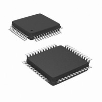
Manufacturer Part Number
M052LAN
Description
IC MCU 32BIT 8KB FLASH 48LQFP
Manufacturer
Nuvoton Technology Corporation of America
Series
NuMicro M051™r
Specifications of M052LAN
Core Processor
ARM Cortex-M0
Core Size
32-Bit
Speed
50MHz
Connectivity
EBI/EMI, I²C, IrDA, SPI, UART/USART
Peripherals
Brown-out Detect/Reset, LVD, POR, PWM, WDT
Number Of I /o
40
Program Memory Size
8KB (8K x 8)
Program Memory Type
FLASH
Ram Size
4K x 8
Voltage - Supply (vcc/vdd)
2.5 V ~ 5.5 V
Data Converters
A/D 8x12b
Oscillator Type
Internal
Operating Temperature
-40°C ~ 85°C
Package / Case
48-LQFP
Lead Free Status / RoHS Status
Lead free / RoHS Compliant
Eeprom Size
-
Available stocks
Company
Part Number
Manufacturer
Quantity
Price
Company:

Part Number:
M052LAN
Manufacturer:
NuvoTon
Quantity:
130
Company:
Part Number:
M052LAN
Manufacturer:
Nuvoton Technology Corporation of America
Quantity:
10 000
Part Number:
M052LAN
Manufacturer:
NUVOTON
Quantity:
20 000


™
NuMicro M051
Series Technical Reference Manual
LIST OF FIGURES
Figure 5.1-1 NuMicro™ M051 Series Block Diagram..................................................................... 17
Figure 5.1-1 NuMicro™ Naming Rule............................................................................................. 19
Figure 5.1-1 NuMicro™ M051 Series QFN33 Pin Diagram............................................................ 21
Figure 5.2-1 NuMicro™ M051 Series LQFP-48 Pin Diagram........................................................ 22
Figure 6.1-1 Functional Block Diagram.......................................................................................... 26
™
Figure 6.2-1 NuMicro M051
Series Power Architecture Diagram ............................................... 29
Figure 6.3-1 Clock generator block diagram................................................................................ 105
Figure 6.3-2 System Clock Block Diagram .................................................................................. 106
Figure 6.3-3 SysTick clock Control Block Diagram...................................................................... 106
Figure 6.3-4 AHB Clock Source for HCLK ................................................................................... 107
Figure 6.3-5 Peripherals Clock Source Select for PCLK ............................................................. 109
Figure 6.3-6 Clock Source of Frequency Divider ......................................................................... 111
Figure 6.3-7 Block Diagram of Frequency Divider ....................................................................... 111
Figure 6.4-1 Push-Pull Output...................................................................................................... 135
Figure 6.4-2 Open-Drain Output .................................................................................................. 136
Figure 6.4-3 Quasi-bidirectional I/O Mode ................................................................................... 137
Figure 6.5-1 I2C Bus Timing ........................................................................................................ 159
Figure 6.5-2 I2C Protocol ............................................................................................................. 160
Figure 6.5-3 Master Transmits Data to Slave .............................................................................. 161
Figure 6.5-4 Master Reads Data from Slave ............................................................................... 161
Figure 6.5-5 START and STOP condition.................................................................................... 162
Figure 6.5-6 Bit Transfer on the I2C bus...................................................................................... 163
Figure 6.5-7 Acknowledge on the I2C bus................................................................................... 163
Figure 6.5-8 I2C Data Shifting Direction ...................................................................................... 165
Figure 6.5-9: I2C Time-out Count Block Diagram........................................................................ 167
Figure 6.5-10 Legend for the following five figures ...................................................................... 178
Figure 6.5-11 Master Transmitter Mode ...................................................................................... 179
Figure 6.5-12 Master Receiver Mode........................................................................................... 181
Figure 6.5-13 Slave Transmitter Mode ........................................................................................ 183
Figure 6.5-14 Slave Receiver Mode............................................................................................. 184
Publication Release Date: Sep 14, 2010
- 6 -
Revision V1.2
Related parts for M052LAN
Image
Part Number
Description
Manufacturer
Datasheet
Request
R

Part Number:
Description:
Manufacturer:
Nuvoton Technology Corporation of America
Datasheet:
Part Number:
Description:
Manufacturer:
Nuvoton Technology Corporation of America
Datasheet:
Part Number:
Description:
Manufacturer:
Nuvoton Technology Corporation of America
Datasheet:
Part Number:
Description:
Manufacturer:
Nuvoton Technology Corporation of America
Datasheet:
Part Number:
Description:
Manufacturer:
Nuvoton Technology Corporation of America
Datasheet:
Part Number:
Description:
Manufacturer:
Nuvoton Technology Corporation of America
Datasheet:
Part Number:
Description:
Manufacturer:
Nuvoton Technology Corporation of America
Datasheet: