AT89LP52-20JU Atmel, AT89LP52-20JU Datasheet - Page 89
AT89LP52-20JU
Manufacturer Part Number
AT89LP52-20JU
Description
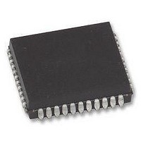
IC MCU 8051 8K FLASH SPI 44PLCC
Manufacturer
Atmel
Series
89LPr
Datasheet
1.AT89LP52-20MU.pdf
(113 pages)
Specifications of AT89LP52-20JU
Core Processor
8051
Core Size
8-Bit
Speed
20MHz
Connectivity
EBI/EMI, I²C, SPI, UART/USART
Peripherals
Brown-out Detect/Reset, POR, PWM, WDT
Number Of I /o
36
Program Memory Size
8KB (8K x 8)
Program Memory Type
FLASH
Ram Size
256 x 8
Voltage - Supply (vcc/vdd)
2.4 V ~ 5.5 V
Oscillator Type
Internal
Operating Temperature
-40°C ~ 85°C
Package / Case
44-LCC (J-Lead)
Processor Series
AT89x
Core
8051
Data Bus Width
8 bit
Data Ram Size
256 B
Interface Type
Serial
Maximum Clock Frequency
20 MHz
Number Of Programmable I/os
36
Number Of Timers
3
Operating Supply Voltage
2.7 V to 5.5 V
Maximum Operating Temperature
+ 85 C
Mounting Style
SMD/SMT
Lead Free Status / RoHS Status
Lead free / RoHS Compliant
Eeprom Size
-
Data Converters
-
Lead Free Status / Rohs Status
Details
Available stocks
Company
Part Number
Manufacturer
Quantity
Price
Company:

Part Number:
AT89LP52-20JU
Manufacturer:
Atmel
Quantity:
110


17.9.4
17.9.5
3709B–MICRO–12/10
ISP Exit Sequence
Serial Peripheral Interface
Figure 17-11. In-System Programming (ISP) Start Sequence
Execute this sequence to exit ISP mode and resume CPU execution mode.
Figure 17-12. In-System Programming (ISP) Exit Sequence
Note:
The Serial Peripheral Interface (SPI) is a byte-oriented full-duplex synchronous serial communi-
cation channel. During In-System Programming, the programmer always acts as the SPI master
and the target device always acts as the SPI slave. The target device receives serial data on
MOSI and outputs serial data on MISO. The Programming Interface implements a standard
SPI Port with a fixed data order and For In-System Programming, bytes are transferred MSB
first as shown in
CPHA = 0) where bits are sampled on the rising edge of SCK and output on the falling edge of
SCK. For more detailed timing information see
1. Drive SCK low.
1. Wait at least t
2. Tristate MOSI.
3. Wait at least t
4. Wait t
The waveforms on this page are not to scale.
XTAL1
XTAL1
MISO
MOSI
MISO
MOSI
RST
SCK
RST
SCK
V
V
SSZ
DD
DD
and tristate SCK.
Figure
SSD
RHZ
.
t
SSD
and bring RST low.
17-13. The SCK phase and polarity follow SPI clock mode 0 (CPOL = 0,
t
RHZ
t
SSZ
AT89LP51/52 - Preliminary
t
Figure
RLZ
HIGH Z
HIGH Z
17-14.
t
STL
HIGH Z
HIGH Z
t
ZSS
t
SSE
89
Related parts for AT89LP52-20JU
Image
Part Number
Description
Manufacturer
Datasheet
Request
R

Part Number:
Description:
Manufacturer:
Atmel Corporation
Datasheet:

Part Number:
Description:
IC MCU 8051 8K FLASH SPI 44VQFN
Manufacturer:
Atmel
Datasheet:

Part Number:
Description:
IC MCU 8051 8K FLASH SPI 44TQFP
Manufacturer:
Atmel
Datasheet:

Part Number:
Description:
IC MCU 8051 8K FLASH SPI 40PDIP
Manufacturer:
Atmel
Datasheet:

Part Number:
Description:
DEV KIT FOR AVR/AVR32
Manufacturer:
Atmel
Datasheet:
Part Number:
Description:
INTERVAL AND WIPE/WASH WIPER CONTROL IC WITH DELAY
Manufacturer:
ATMEL Corporation
Datasheet:
Part Number:
Description:
Low-Voltage Voice-Switched IC for Hands-Free Operation
Manufacturer:
ATMEL Corporation
Datasheet:
Part Number:
Description:
MONOLITHIC INTEGRATED FEATUREPHONE CIRCUIT
Manufacturer:
ATMEL Corporation
Datasheet:
Part Number:
Description:
AM-FM Receiver IC U4255BM-M
Manufacturer:
ATMEL Corporation
Datasheet:
Part Number:
Description:
Monolithic Integrated Feature Phone Circuit
Manufacturer:
ATMEL Corporation
Datasheet:
Part Number:
Description:
Multistandard Video-IF and Quasi Parallel Sound Processing
Manufacturer:
ATMEL Corporation
Datasheet:
Part Number:
Description:
High-performance EE PLD
Manufacturer:
ATMEL Corporation
Datasheet: