Morph-IC-II FTDI, Morph-IC-II Datasheet
Morph-IC-II
Specifications of Morph-IC-II
Available stocks


Related parts for Morph-IC-II


Morph-IC-II Summary of contents
Page 1
... Future Technology Devices International Ltd. Document Reference No.: FT_000198 Morph-IC- compact, yet powerful FPGA module which is capable of synthesising LSI (Large Scale Integration) designs using the embedded Altera Cyclone-II FPGA. Communication between the FPGA and carried out via the FTDI FT2232H, a USB 2.0 Hi-Speed (480Mbit/s) USB bridge. Sub-100ms FPGA programming/re-programming makes Morph-IC-II ideal for applications which require users to reconfigure hardware functionality „ ...
Page 2
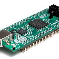
... For example the I/O can be operated at 1.5V/1.8V/2.5V/3.3V. This provides added flexibility to the designer. Morph-IC-II is shown in Fig. 1. The module has 4 connectors giving access to all the FPGA I/Os plus a JTAG header, that can be used to interface to Morph-IC-II with SignalTap Analyser (a function included in the Quartus-II package). SignalTap can be used to display the waveform of every pin of the FPGA. ...
Page 3
... Configuring the Jumper settings....................................................................................... 6 3.2.2 Configuring the FPGA .......................................................................................................... 6 3.3 Morph-IC-II Signal Levels Supported. ................................................................ 7 3.4 Morph-IC-II Header Connections. ....................................................................... 8 3.5 Morph-IC-II Hardware Configuration ................................................................ 14 3.5.1 Communications and Programming Interfaces of Morph-IC-II .............................................. 14 3.5.2 GPIO Connections .............................................................................................................. 16 3.5.3 Morph-IC-II JTAG Connections ....................................................................................... 16 3.5.4 Pin-Map Configuration ....................................................................................................... 17 MorphIO-II – An Application Software ................................................ Electrical Details ...
Page 4
... Providing a fast and easy alternative to ASIC solutions for low to medium volumes of product. Academic FPGA design exercise – ideal for learning and experimenting with HDL (Hardware Design Language) Digital signal processing Audio/Video Cryptography Copyright © 2010 Future Technology Devices International Limited Document Reference No.: FT_000198 MORPH-IC-II Datasheet Version 1.03 Clearance No.: FTDI# 164 3 ...
Page 5
... JTAG interface for testing the I/Os and registers of the FPGA 1 dedicated external clock input 2.1 Driver Support Morph-IC-II uses the FTDI Ft2232H USB bridge chip. This chip requires USB drivers which can be downloaded free of charge from http://www.ftdichip.com/FTDrivers.htm. Royalty free VIRTUAL COM PORT (VCP) DRIVERS for... ...
Page 6
... Functional Description 3.1 Morph-IC-II Block Diagram A block diagram of the Morph-IC-II is given in Fig. 2. Morph-IC-II module can be USB powered or self powered. The power mode is selected using the “VBUS” jumper - as indicated on the diagram below. The FPGA can be programmed from a PC via the USB interface and the FT2232H USB bridge. ...
Page 7
... The Morph-IC-II package includes a *.RBF loader programme called “MorphLd”. This programme is used to load RBF files into the FPGA of Morph-IC-II via the USB to Passive Serial interface. These *.RBF are synthesised HDL (VHDL or Verilog) code with additional settings for the FPGA specified by the Quartus-II options ...
Page 8
... Morph-IC-II Signal Levels Supported. Morph-IC-II provides a flexible method to process signals of different voltage levels. This method allows a voltage of either 3.3V, 2.5V, 1. applied to I/O Bank 4 by adjusting the externally supplied power supply to bank 4 and reconfiguring the pin-map. This means Morph-IC-II supports the different voltage levels on different banks as shown in Fig illustrated in Fig. 3 I/O Banks 1 – ...
Page 9
... Morph-IC-II Header Connections. Morph-IC-II‟s FPGA is connected to five connectors: J1-J4 and the JTAG Port are used for the following functions: connecting I/Os, “self-powered” power supply, specific bank supply voltages and clock connections. The JTAG connector is used to scan the I/O and registers of the FPGA. ...
Page 10
... Low) J1-31 J1-32 J1-33 J1-34 J1-35 J1-36 J1-37 J1-38 J1-39 J1-40 Table 3 – Pin out of Connection J1 Document Reference No.: FT_000198 MORPH-IC-II Datasheet Version 1.03 Clearance No.: FTDI# Name Description IOR3 General Input/output IOL3 General Input/output GND 0V Power pin GND 0V Power pin IOL4 ...
Page 11
... J2-29 J2-30 J2-31 J2-32 J2-33 J2-34 J2-35 J2-36 J2-37 J2-38 J2-39 J2-40 Table 4 – Pin out of Connection J2 Document Reference No.: FT_000198 MORPH-IC-II Datasheet Version 1.03 Clearance No.: FTDI# Name Description IOA6 General Input/Output IOB7 General Input/Output GND 0V Power pin GND 0V Power pin IOG7 ...
Page 12
... J4-13 J3-14 J4-15 J4-16 J4-17 J4-18 J4-19 J4-20 J4-21 J4-22 J4-23 J4-24 Table 6 – Pin out of Connection J4 Document Reference No.: FT_000198 MORPH-IC-II Datasheet Version 1.03 Clearance No.: FTDI# Name Description IOR14 General Input/Output ION14 General Input/Output IOP16 General Input/Output IOP15 General Input/Output ION16 ...
Page 13
... GND GND IOM4 IOG7 IOK4 IOG6 3V3IO V_BANK4 IOK5 IOD5 ION8 IOE6 GND GND IOR8 IOF9 IOM11 IOC12 Fig. 4 – Pin outs of J1 & J2 Document Reference No.: FT_000198 MORPH-IC-II Datasheet Version 1.03 Clearance No.: FTDI# Morph-IC II Pin-out J2 (Top View) AD2 1 2 AD1 IOE3 ...
Page 14
... Copyright © 2010 Future Technology Devices International Limited Document Reference No.: FT_000198 Morph-IC II Pin-out Variable Voltage Lines Lines IOF15 IOH13 IOG12 IOJ11 IOJ12 IOB12 IOB13 IOB14 IOD15 IOE14 GND JTAG_TDO MORPH-IC-II Datasheet Version 1.03 164 Clearance No.: FTDI# J4 (Top View) IOD13 1 2 IOD14 3 4 IOG13 5 6 IOC14 7 8 ...
Page 15
... This mode can transmit data at higher rates than asynchronous 245 FIFO. These signals are only available on channel A of the FT2232H chip therefore; Morph-IC-II uses channel A for the FIFO interface as opposed to MorphIC-1K which has the FIFO interface in channel B. This leaves channel B available on Morph-IC- used to program the FPGA ...
Page 16
... Fig. 7 – The 245 Communication Interface Copyright © 2010 Future Technology Devices International Limited Document Reference No.: FT_000198 Communications Interface AD0 AD1 AD2 AD3 AD4 AD5 AD6 ALTERA CYCLONE II AD7 IO EP2C5F256C8N RXF TXE RD WR SI/WUB CLKOUT OE MORPH-IC-II Datasheet Version 1.03 164 Clearance No.: FTDI# FPGA 15 ...
Page 17
... USB 3.5.3 Morph-IC-II JTAG Connections The interface between a JTAG programmer and Morph-IC-II‟s JTAG interface is illustrated in Fig. 9. The block on the left represents a programmer that will interface with the Morph-IC-II. The block on the right represents the Morph-IC-II FPGA module. JTAG Programmer Copyright © 2010 Future Technology Devices International Limited ...
Page 18
... Pin-Map Configuration The Cyclone-II FPGA of the Morph-IC-II can be configured from an *.RBF file. These *.RBF files can be generated using the free software package called Quartus II. An *.RBF file generated by Quartus II contains the *.RTL code which synthesises the circuit, the signals of each pin (which are defined in the top level entity of the * ...
Page 19
... MorphIO- easy to use utility used for displaying and setting the binary levels and port direction of all Morph-IC-II‟s 80 I/Os. A screen shot demonstrating how the IO are set is given in Fig. 10. This diagram shows MorphIO-II with some voltage levels set to different values. An illustration of J1-19 being set to low and J1-15 being set to high is also shown here ...
Page 20
... Fig. 11 – MorphIO-II User Interface Fig. 12 – Set Clock Frequency Copyright © 2010 Future Technology Devices International Limited Document Reference No.: FT_000198 MORPH-IC-II Datasheet Version 1.03 Clearance No.: FTDI# 19 164 ...
Page 21
... Electrical Details 5.1 Absolute Maximum Ratings The absolute maximum ratings of Morph-IC-II are as follows. Exceeding these values may cause permanent damage to the device. Parameter Storage Temperature Ambient Operating Temperature (Power Applied) DC Input Voltage – USBDP and USBDM DC Input Voltage – All Other Inputs such as ...
Page 22
... Copyright © 2010 Future Technology Devices International Limited Minimum Typical Maximum - 0.80 2.00 - 1.50 0.80 1.10 - 1.60 2. 190 40 75 190 Document Reference No.: FT_000198 MORPH-IC-II Datasheet Version 1.03 Clearance No.: FTDI# Units Conditions V LVTTL V LVTTL V LVTTL V V KΩ Vin = 0 KΩ Vin =VCCIO KΩ 3.3V CCIO 21 164 ...
Page 23
... Mechanical Details The mechanical details of Morph-IC-II are illustrated in Fig. 13. 16.8mm 10mm Fig. 13 – Morph-IC-II Dimensions (Top and Side View) All dimensions shown in millimetres with a tolerance of ±0.1mm. The headers J1, J2, J3 and J4 are mounted on the bottom of the PCB. The overall height (top of USB connector to bottom of pins) of the module is 18 ...
Page 24
... Copyright © 2010 Future Technology Devices International Limited sales1@ftdichip.com support1@ftdichip.com admin1@ftdichip.com http://www.ftdichip.com http://www.ftdichip.com tw.sales1@ftdichip.com tw.support1@ftdichip.com tw.admin1@ftdichip.com http://www.ftdichip.com us.sales@ftdichip.com us.support@ftdichip.com us.admin@ftdichip.com http://www.ftdichip.com cn.sales@ftdichip.com cn.support@ftdichip.com cn.admin@ftdichip.com http://www.ftdichip.com Document Reference No.: FT_000198 MORPH-IC-II Datasheet Version 1.03 Clearance No.: FTDI# 23 164 ...
Page 25
... Disabled Table 5 - Default Internal EEPROM Configuration The EEPROM on the Morph-IC-II can be re-programmed over USB using the utility program MPROG or FT_PROG. Both can be downloaded from the www.ftdichip.com. MPROG Version 3.5 or later is required for the FT2232H chip. Users who do not have their own USB Vendor ID but would like to use a unique Product ID in their design can apply to FTDI for a free block of unique PIDs ...
Page 26
... First draft Rev 1.0 First release Rev 1.01 Minor text corrections Rev 1.02 Updated max speed to 40Mbytes/s due to new driver Rev 1.03 Added a note on the MORPHPROG.dll not being supported by Windows CE Copyright © 2010 Future Technology Devices International Limited th 28 October 2009 9 th ...
Page 27
Appendix C – Schematic Drawings Copyright © 2010 Future Technology Devices International Limited Fig. 14 – A Schematic of the USB Interface 26 ...
Page 28
Fig. 15 – A Schematic of the FPGA Copyright © 2010 Future Technology Devices International Limited 27 ...
Page 29
Fig. 16 – A Schematic of the I/O Pin Copyright © 2010 Future Technology Devices International Limited 28 ...
Page 30
Appendix D - Assembly Drawings Copyright © 2010 Future Technology Devices International Limited Fig. 17 – Component Layout Top View Fig. 18 – Component Layout Bottom View 29 ...