Morph-IC-II FTDI, Morph-IC-II Datasheet - Page 18
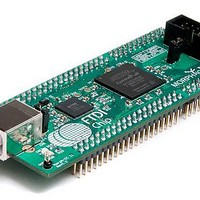
Morph-IC-II
Manufacturer Part Number
Morph-IC-II
Description
Interface Modules & Development Tools USB Hi-Speed Altera Cyclone-II FPGA Mod
Manufacturer
FTDI
Datasheet
1.MORPH-IC-II.pdf
(30 pages)
Specifications of Morph-IC-II
Interface Type
Programmable
Data Bus Width
Serial, 8 bit
Operating Supply Voltage
5 V
Product
Interface Modules
Features
Ultra Fast FPGA Configuration, JTAG Interface
Core Architecture
Cyclone
Core Sub-architecture
Cyclone II
Kit Contents
Board
Kit Features
FT2232HQ Dual, Hi-Speed USB UART/FIFO IC Used For USB
For Use With/related Products
FT2232H, EP2C5F256C8N
Lead Free Status / RoHS Status
Lead free / RoHS Compliant
Available stocks
Company
Part Number
Manufacturer
Quantity
Price


Document Reference No.: FT_000198
MORPH-IC-II Datasheet
Version 1.03
164
Clearance No.: FTDI#
`
3.5.4 Pin-Map Configuration
The Cyclone-II FPGA of the Morph-IC-II can be configured from an *.RBF file. These *.RBF files can be
generated using the free software package called Quartus II. An *.RBF file generated by Quartus II
contains the *.RTL code which synthesises the circuit, the signals of each pin (which are defined in the
top level entity of the *.RTL) and the settings of each pin (which includes current draw and logic level
standards). The pin map editor included in Quartus-II is used to specify the signal assignments and the
setting of each pin.
Along with making pin assignment to each port of the top-level entity, the voltage and current can be
defined for each port. However there are restrictions, every signal in an I/O Bank needs to operate at the
same logic voltage level and the I/O Bank needs to be powered with the same voltage as the logic
voltage level of the signals. Morph-IC-II‟s I/O Banks 1 to 3 are connected directly to the FT2232H chip
and all these signals are fixed to 3.3V-TTL/CMOS. I/O Bank 4 is the only bank that can have signals
operating at voltages other than 3.3V-TTL/CMOS. Again all signals need to be at the same logic voltage
level, to supply power with a voltage other than 3.3V, remove V_BANK4 jumper and apply DC power
regulated to the same voltage level as the logic voltage level of I/O Bank4 to (at least one of) the header
nodes labelled V_BANK4. More information and an example for pin-map editing are given in the
application note: AN_141_MorphIO-II and MorphLd Utilities for Morph-IC-II
Copyright © 2010 Future Technology Devices International Limited
17
Related parts for Morph-IC-II
Image
Part Number
Description
Manufacturer
Datasheet
Request
R

Part Number:
Description:
Interface Modules & Development Tools Obsolete See MORPH-IC-II
Manufacturer:
FTDI
Datasheet:

Part Number:
Description:
MODULE USB TO FPGA
Manufacturer:
FTDI, Future Technology Devices International Ltd
Datasheet:

Part Number:
Description:
BOARD, EVALUATION, UK PSU
Manufacturer:
FTDI
Datasheet:
Part Number:
Description:
BOARD, EVALUATION, US PSU
Manufacturer:
FTDI
Datasheet:
Part Number:
Description:
Specifications: Manufacturer: FTDI ; Product Category: USB Interface IC ; RoHS: Details ; Operating Supply Voltage: 3 V to 5.25 V ; Supply Current: 25 mA ; Maximum Operating Temperature: + 70 C ; Mounting Style: SMD/SMT ; Package / Case: QFN-32
Manufacturer:
FTDI
Part Number:
Description:
integr. usb2.0/uart lqfp32 rohs ftdi reel c1k...
Manufacturer:
FTDI
Datasheet:
Part Number:
Description:
Interface Development Tools USB to UART Breakout Board
Manufacturer:
FTDI
Datasheet:

Part Number:
Description:
IC USB TO SERIAL UART 32-QFN
Manufacturer:
FTDI, Future Technology Devices International Ltd

Part Number:
Description:
USB Interface IC USB to Serial UART Enhanced IC SSOP-28
Manufacturer:
FTDI
Datasheet:

Part Number:
Description:
IC, USB UART INTERFACE, SSOP-28
Manufacturer:
FTDI
Datasheet:

Part Number:
Description:
IC, USB UART INTERFACE, QFN-32
Manufacturer:
FTDI
Datasheet:
Part Number:
Description:
IC, USB FIFO INTERFACE, SSOP-28
Manufacturer:
FTDI
Datasheet:
Part Number:
Description:
MODULE, USB, 4 PORT, FT4232H BASED
Manufacturer:
FTDI
Datasheet:
Part Number:
Description:
357-036-542-201 CARDEDGE 36POS DL .156 BLK LOPRO
Manufacturer:
FTDI
Datasheet:
Part Number:
Description:
357-036-542-201 CARDEDGE 36POS DL .156 BLK LOPRO
Manufacturer:
FTDI
Datasheet: